The Premise
Now heads up, I’ve not finished yet, I still have a bunch of stuff to do, but heres the gist of things. My partner stumbled onto a game called Turing Complete that I’ve played a lot of recently. From the broadest possible overview of what this game is, basically you start from nothing but a NAND gate, and have to first produce the logic gates, then a few components such as a latch and a full adder, and then you have to expand that up to 8 bit components, until ultimately you end up building a computer using nothing but the gates and components you’ve produced previously, and it makes doing so super intuitive I’m genuinely a fan of how this game teaches bare metal computing. Of course I do have some issues with it such as it disallowing monostable circuts, but thats besides the point for now
(though this did fuck up my ability to try and recreate a 6502 processor from a circuit diagram I found which relies on a monostable circuit to do its BCD arithmetic, but again, thats not what I’m here to ramble on about)
So heres the premise. On Monday, so a couple days before writing this, I learned that the game has a neat little component called a “6×8 Dot Matrix Display” module, but thats a mouthful so I’m just calling them “Screens”. I’m told that this screen was originally intended for character drawing, like letters and stuff, but I decided to be a little bit of a smart arse about it and see how far I can push this thing.
I’m gonna assume if you’re reading this, you’re already comfortable with the concept of bits, bytes, the fact that the lowest bit is the last one, etc. When I use the syntax “Bx.y”, I mean the y-th bit of byte x, where B0.0 is the lowest bit and B3.7 or B7.7 is the highest bit of 32 and 64 bit inputs.
6×8 Screen Modules
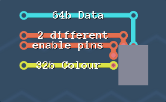
On its surface the screen is very simple, if a little bit opaque.

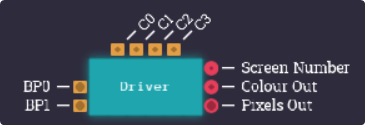
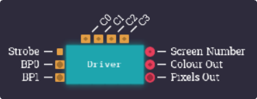
A single screen has 4 input pins.
- First is a 64 bit data line. This serves 2 purposes, the middle 6 bytes of the data tells the screen what pixels to write, and if the 56th bit (B8.0) is set, then it will “flush” the screen, and all the updates made to it will display all at once.
- Second is a pair of enable pins. There is one next to the data line, and one next to the colour line. In order for the screen to update, both of these pins need to be enabled.
- Lastly there is a 32 bit colour line. The top three bytes are the red, green and blue components, where 0 is completely off and 255 is completely on.
Now, how do these screens update? Firstly you need to set the pixels that you want to update on the data line, and the colour that you want those pixels to be on the colour line, and then you can turn on both of the enable pins and those pixels will update. There is no way to set different pixels to different colours during a single tick, and this will cause some issues for us later. If a pixel isn’t selected on the data line, that pixel does not change. Once we’ve done all our different colour writes, we can then send just $0100 0000 0000 0000 down the data line. The colour doesn’t matter and can stay 0, then we can enable the screen, and the screen will flush all the changes and update.
This means that we can essentially paint a picture on the screen one colour at a time, update it all at once, and then on the next frame, paint over the first picture.
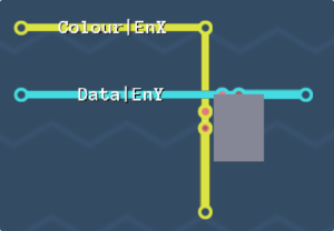
Now thats all well and good, but how on earth are we meant to do anything with just 48 pixels? Well you know how I said that data uses the middle 6 bytes and colour the top 3? There is a really important reason for that:
In Turing Complete, only the lowest bit(s) of a line are read into an input pin if the input pin has a smaller width than the line it’s connected to. This means that we can run both the data/colour and the enable through the same wire, and also explains why we need to set two enable pins high to update a circuit!
Now we just need a grid of these screens, some way to select which row and which column to enable, and we’ll be good to go. Bonus points, the game threw us a bone on this one. The right and bottom edges of the screen float slightly above the wires layer, meaning that they don’t interfere with our ability to draw wires.
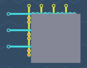
Suddenly, we have a grid!
How cool is that? Now this grid is 24 pixels wide, and 24 pixels tall, which is good! Our ultimate end goal is to make a PPU, and that means we have to work in 8×8 pixel characters. What’s a tad frustrating about it though is that its 4 screens wide, not 3. That makes a lot of what comes next a lot harder to tackle.
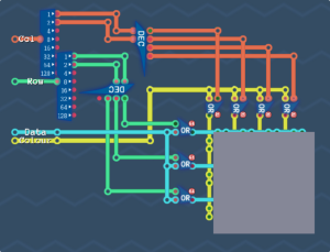
Oh and for completeness sake, lets add a few extra gates, and finish up this screen so that we can see what it wants to look like. A couple of OR gates to append an enable signal to the row or column will get the job done.
Just a brief explainer.
- That chip on the left with the arrows is a splitter. A byte splitter takes a single 8 bit input and outputs 8x 1 bit inputs. There are also versions for 16/32/64bit that takes the input and returns 2/4/8 bytes. There are also makers that take the input bits/bytes and output the relevant cable widths.
- The middle blue chip with DEC on it is a decoder. there are 1, 2 and 3 bit variants that take 1, 2 and 3 bits as input, and outputs exactly one out of 2, 4 or 8 lines depending on the combination on the input. The 3 bit decoder also has a disable pin that prevents any output line from enabling. This will be useful later.
So as you can see, we’re simply ORing the enabled row and column into the colour and data, and that means that while all the screens get the colour and data, only the specific screen in the enabled row and column will be updated with it.
Tiles and Bitplanes
Now that we have the set up, let me explain what my actual goal of this whole mess is to do.
I want to create a picture processing unit that can take an 8×8 tile of 2 Bits Per Pixel (bpp) graphics, and output it to the screen.
I’m not going to worry about trying to reposition these tiles (yet), and I’m also going to assume (for the time being) that the screen array has a width that is a multiple of 4 screens. This means that my input data can have rows that are a multiple of 3 tiles, and all will be good.
The reason that I’m making these assumptions is because, as you may have guessed, I’m trying to draw 8×8 tiles onto 8×6 screens, and thats going to be a heck of a lot easier said than done. Not counting the time I’ve spent getting screenshots for this post, I’ve spent 14 hours so far trying to build this and it’s still buggy and incomplete.
While I’d like to talk more about the end goal, lets start with the immediate task at hand. How do I define my data, and what can I do to get it onto a screen. First lets consider the exact data that I’m wanting to use. My graphics are going to ultimately be 8×8 pixel “characters” (or tiles) which each have 4 different colours: 00, 01, 10 and 11.
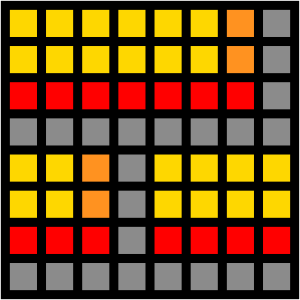
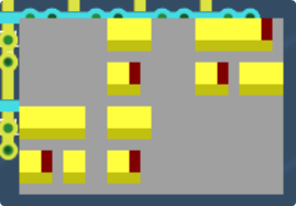
Lets use this brick block on the right as an example. The colours look a little bit jank, but it’ll make it easier to see whats going on.
Now we should first define our palette to see whats going on, lets call the grey 00, the red 01, the orange 10, and the yellow 11. I’ll add these to our drawing of the brick block now.
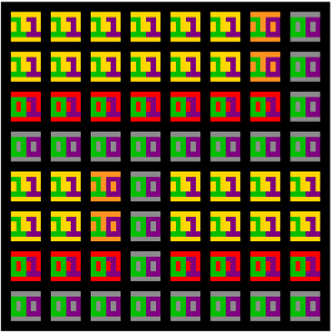
Now rather suggestively, you may have noticed that in each pair, I’ve made the first and second bits different colours. This is where the magic trick happens. If we break down our 2bpp tiles into 2 1bpp tiles called “bitplanes” and you can find out more about them here. If we get our graphics down to a single set of 8 bytes, we’ll be able to work with them more easily in future, so now I’m going to pull out each of these bitplanes so that we can see what our tile really looks like.
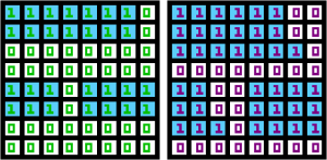
So we now have two different sets of 64 bits. The one on the left is Bitplane 1 (as it is bit 1 of each of the colours) and the right one is Bitplane 0 (the 0th bit of each colour.)
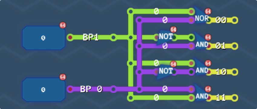
We can also recover the colours we need with a bit of simple logic.
¬(A+B) = 00, Grey. A*B = 11, Yellow. ¬A*B = 01, Red, and A*¬B = 10, Orange, where A is BP1 and B is BP0. That logic is displayed in the picture below.
Creating a Graphics Driver
Now building a PPU comes in basically two steps. First is a way to get tile data into a graphics driver that can control these blasted screens, and second is the graphics driver that controls these blasted screens.
I’m going to work backwards, that seems easier, so lets start with the graphics driver.
Here’s at the most basic level what we want.
A chip that somehow takes our two bitplanes, our four colours, and outputs which screens to update with what.
Now first, a few things to note: Since we need to output each individual colour to each individual screen, that means every tile is going to take some greater than 1 number of ticks to draw, so we can’t just pump data into this thing as fast as we can, as it’ll be throttled by the speed of the output.
But we also can’t trust that the actual tile data will always be on the input line for those entire 8 ticks, so we need some way to tell the chip that it needs to start drawing a new tile.
That’ll make things easier. When we have our data on the input pins and ready to go, we’ll be able to set the strobe high for a tick, and that’ll make it so that our chip can quickly save all the input values, and then do its magic.
Now lets have a think about what our chip needs to do.
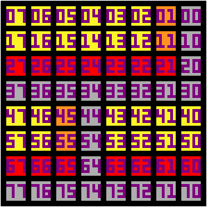
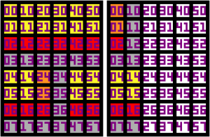
There are two main issues with preparing the data for being output. firstly, the input data is coming in as 8 bytes, where each byte is a row of the tile, the first byte (which ultimately comes from memory, so we can define how those are passed around internally however we want) being the top row, and so on. For our purposes, we’ll call the top row the highest byte, though in hindsight it’d have been simpler to have the top row be the lowest byte. I’ll write what bit each tile is on our brick graphic to the right, the top left 07 represents B0.7.
Just for testing I’ll take a little detour and show how this data could be read into the chip using some 8-bit buffers to store values read from a RAM chip.
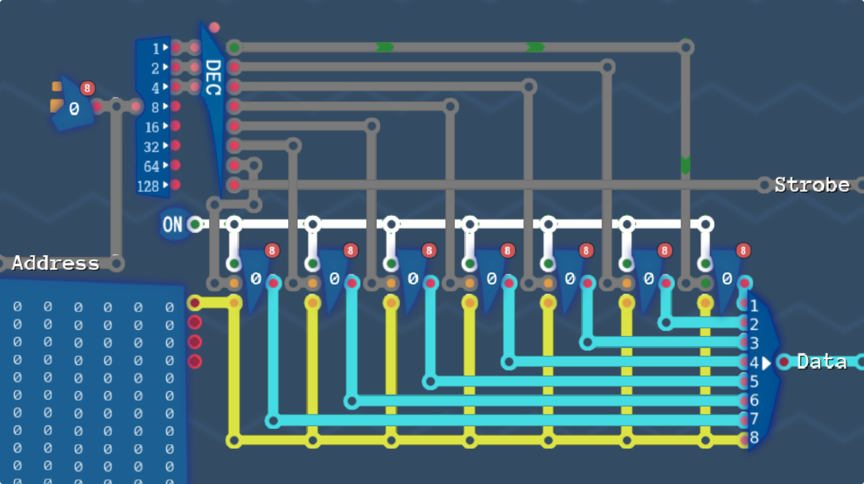
There are a fair few new components to explain here, so let me have a crack at it. The DEC as I explained above is a decoder, just this is the 3 bit variant. The triangle ones in the middle with 3 inputs and an output is a register. The three inputs are Read, Write, and Data, and the output is Data. We always want Read to be high, and the decoder at the top selects a specific register to write to. On the far left is a RAM chip. Out of frame is its address and read pins, which would select a cell and output that byte onto the line. In the top left is a counter. This just increments every tick. The pins are for manually setting the value of it (something for program jump control, but we don’t care here.) So what happens is that on tick 0, it reads address 0 into the last buffer, then tick 1 reads address 1 into the second to last buffer, all the way up to tick 7, where all 7 buffers have the previous 7 bytes of data, the last byte is on the yellow line, so we can set the strobe high and send all 8 bytes to our driver at once.
Anyways, now that we know what our input data looks like, lets check what the screens expect our output to look like… Oh. Right, I need to split the tile across two different screens.
That aside, lets look at how each tile lines up on the screen. Our B0.7 needs to become B0.0, our B7.7 needs to become B0.7, and so on. If we treat the second screen as B6 and B7, we can see that what we have to do is rotate the input data counter clockwise to make sure it maps properly.
Personally I implemented this using 2 seperate simple chips, one that transposes the data (so the top would still be B0.7, but now the top row is all the bit 7s and the bottom row is all the bit 0s, with the bytes in descending order), and then a second that reverses the order of the bytes in a 64 bit line. Because the game doesn’t have a delay score for cable un/packing, these transpositions are free operations anyway, though I suspect it might be a tiny simulation optimisation to implement a single rotate chip anyway.
Now that we know what our data coming in looks like, what the outgoing data looks like, and roughly how we are going to do it, lets take a look at the chip we want to build shall we?
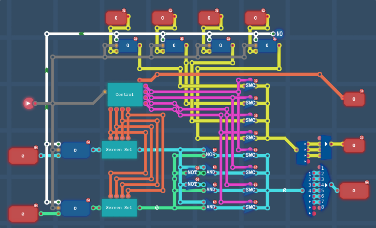
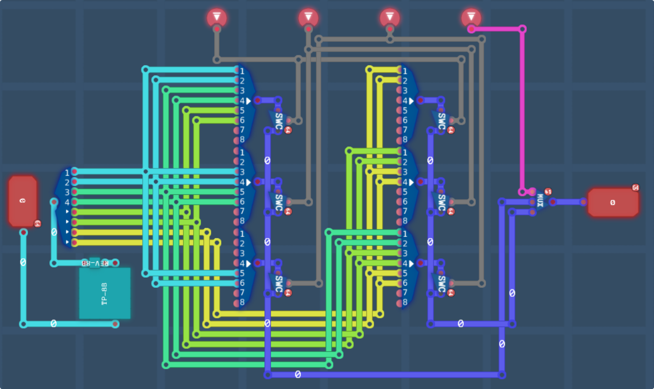
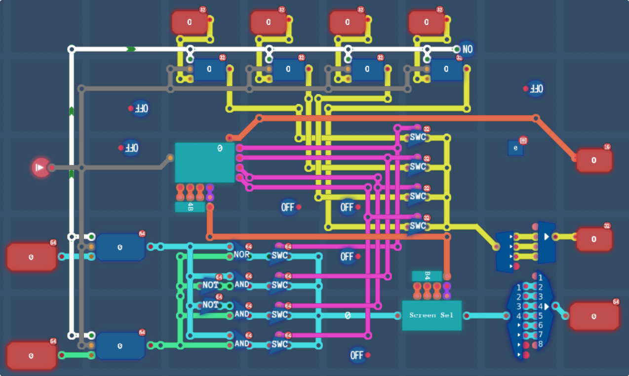
Few more bits to explain before we get started. As with all chips, the red tiles are the inputs and outputs. Here our inputs on the left are “Strobe”, “BP0” and “BP1”, and on the top, the inputs are “Colour 0” through “Colour 3”. On the right, the outputs are “Screen Number”, “Colour” and “Data.” As explained above, the driver is only going to take the input tiles and convert them to screens. It doesn’t need to care about how large the screen array is, or how many tiles are in each row. That is a job that can be left to someone outside this chip.
The dark blue boxes are registers. They work exactly the same as the 8 bit register, just these are 32 and 64 bit. The read pin is set to always on by the constant 1 on the white line. The write bit is wired directly into the strobe line. This is how our chip is going to snapshot the input data at the start of a drawing cycle and remember it until the end.
In the middle, the chips marked SWC are switches. They take the incoming data, and only send it to the outgoing pin if the side pin is enabled. This is how we can have 4 different values being output onto the same line.
Now this is all well and good, but we have a slight issue, those two cyan magic chips, “Screen Sel” and “Control.” Thats what takes this from a 10 minute wiring job into a 7 hour testing phase.
The First Attempt at a Driver
Now, lets focus on the two magic chips, as between my first and second attempt at making a driver, only these two chips changed.
The “Control” chip is the brains of the operation. It’s what is going to keep track of the whole drawing procedure, as well as where on the screen array the data is being written to, and also what colours and screens to write to the screens on a given tick. In my actual run through building this chip, the logic that should have been in this chip is instead just strewn around the Driver chip. At the end of the day it does exactly the same thing, just packaging it all up is slightly neater.
If the control chip is the brains, then the “Screen Sel(ect)” chip is the muscles. This takes a screen number from the control chip and outputs the data that needs to be drawn to that specific screen. Again, in my original run of the driver, this logic was just embedded onto the driver chip instead of bundled away (though I did bundle it in round two, but we’ll get there later.)
Heres the methodology that I used the first time I made this driver chip. And if it’s not obvious, something here went wrong, I’ll leave it to you to see if you can figure it out before the next chapter.
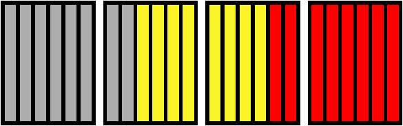
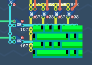
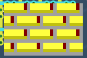
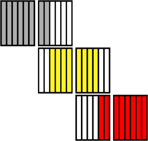
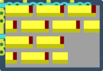
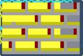
Now. Here is my logic for how I built the screen select chip. I knew that I needed to be able to read in 3 tiles (which was 3 pulses of the strobe line) and that I then needed to output 4 screens. As you can see in the diagram to the right (where each column is 1 byte, so 6 columns is 1 screen,) the first screen is comprised entirely of the first tile; the second screen has the last two bytes of the first tile, and the first half of the second tile; the third screen has the second half of the second tile, and the first 2 bytes of the third tile; and the last screen is composed entirely of the last tile’s bytes.
Seeing this pattern, my first instinct would be to save the last 2 bytes of the first tile, and the last 4 bytes of the second tile, then use those bytes in conjunction with the buffered input coming into the chip to generate all 6 bytes of the screen, which I could then output at once.
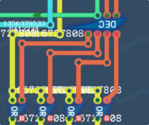
This would mean that on the first strobe, screen 1 would be written. On the second strobe, screen 2 would be written, and on the final strobe, both screen 3 and 4 would be written back to back. Let me show you what this chip looks like.
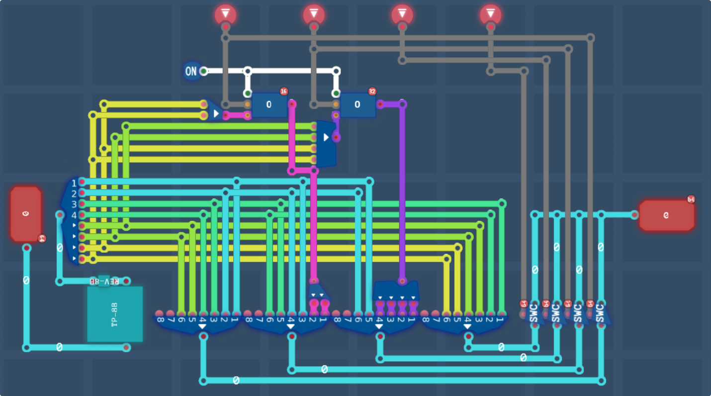
Nothing too majorly complicated (though I wired it a hell of a lot cleaner here than I did before lol.) Very first thing is to rotate our rows into columns, which is what “TP-8B” (TransPose 8 Bytes) and “REV-8B” (REVerse 8 Bytes) do.
On screen 1, we want to write to the 16 bit buffer capturing the top 2 bytes of the input tile, which for screen 1 will always be tile 1. These are then output to the packer for screen 2. On screen 2, we know that the incoming tile is tile 2, so we buffer the top 4 bytes of the tile and output it to screen 3. Screen 1 and 4 are just the bottom and top 6 bytes of the input, and then at the end we have a set of switches that only allows the specific screen’s input to pass through. Simple enough, means we can now take a stream of tiles and output them as a set of screens.
Next challenge, the control chip, and I’ll admit, I wish I had written this blog as I was building this first time, instead of after, as trying to decypher the mess of strewn about wires is a bit of a pain. Don’t worry I’ll show you the mess at the bottom of the chapter so that you can look upon me and gasp in horror and/or fear.
So we need to do 3 things in a control chip:
- Wait for the strobe signal
- Write to each screen 4 times, incrementing the colour index each time.
- Write up to 4 screens every 3 strobes.
While complex, this is reasonably doable. Bonus points, I can skip most of the debugging now that I know what the logic is supposed to look like (at least 3 of the 7 hours I spent on this chip was just hardware debugging.)
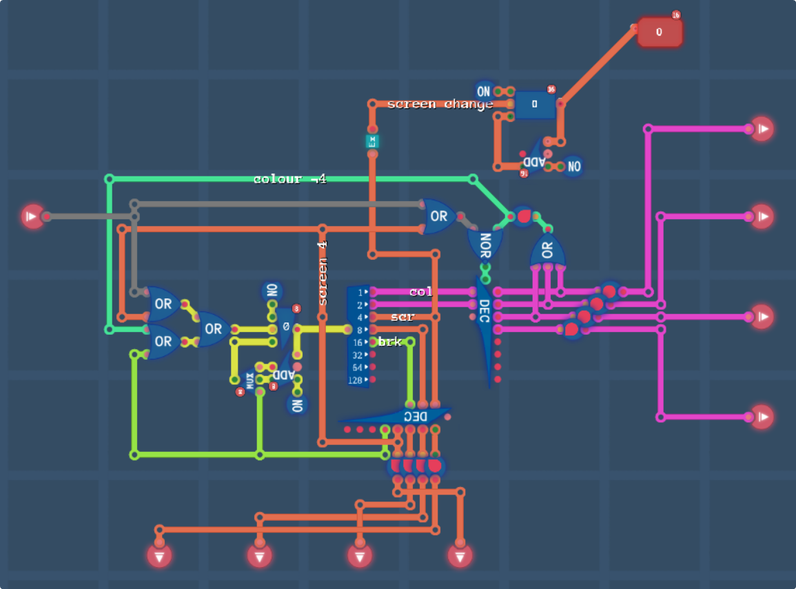
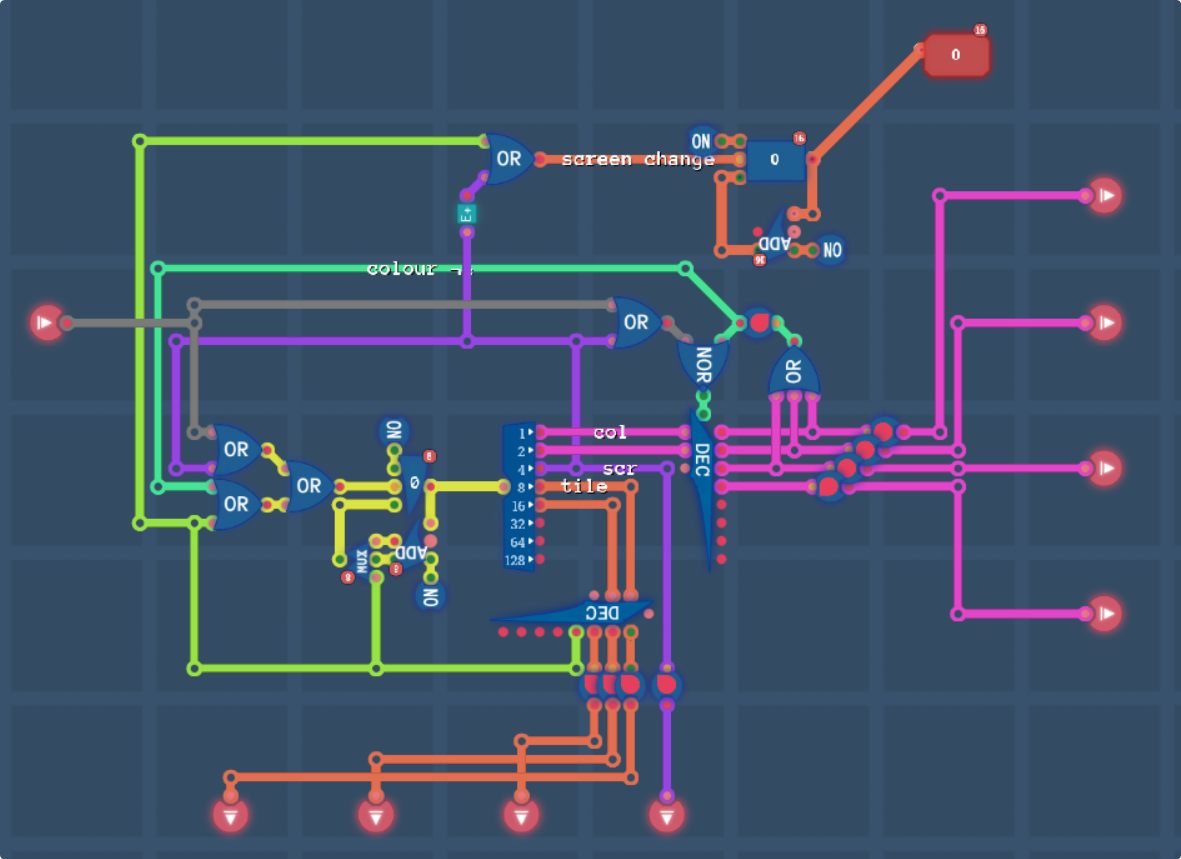
Now this one has a lot more going on. The first thing of note is the two loops which consist of a register, an adder and a multiplexer (though in hind-sight I could have used a switch here, since an empty line is treated as a 0 instead of a third state in this simulation, but lets call it realism or something idk.) These are counter constructions.
While the game does have a built in counter module, the counter always increases every tick, which is unsuitable for what we need. We need a counter that only increments when we let it, and when we let it is controlled by the “Screen change” line in the case of the screen number counter, or that stack of OR gates on the left for our cycle counter.
We know that when we need to draw a screen, we need to draw 4 colours, and then move on to the next screen, so lets talk about the cycle counter. It’s going to tick up every time we want to draw something, and when we do want to draw, we’re going to draw 4 colours to one screen, then move on to the second screen and draw the next 4 colours, and then the third and fourth screen.
4 colours x 4 screens is 16 cycles, but for our purposes, 4 is a power of 2, which means we can divide using just the number of bits.
This means that the bottom 2 bits of our counter can represent the colour we want to output, the next two bits can be the screen number, and if we roll over into the 5th bit, we know we’re done with the current set of tiles, so we can reset our counter.
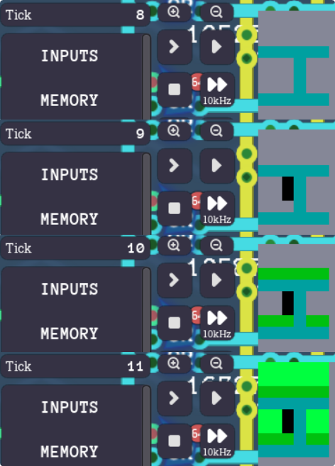
I think the easiest way to explain how the chip works is by starting with a strobe and seeing what happens.
The first thing that happens is that the strobe enables the colour output decoder by tripping the NOR gate just above. This allows colour 0 through the decoder, which is sent to the output, and also goes into a delay chip just above. The strobe also enables the write signal of our cycle counter.
On the second tick, the strobe is no longer high, so we need another way to keep the counter moving. The delay chip above the colour decoder though is now outputting high, because one of its inputs was high on the previous cycle. This is how we’ll keep the counter high, the decoder enabled, and keep things moving. The same happens on the third tick.
On the fourth tick, the decoder outputs colour 3, which isn’t connected to the delay circuit, so it no longer holds the delay circuit high. Nothing is going to happen just yet, but on the next tick this will shut everything down until the next strobe. Colour will be back to 0, and the screen number will go from 0 to 1.
At the top of the circuit is a small chip labeled “Ex”. This is a tiny custom edge detector that I built (I also have “E+” and “E-” as rising and falling edge detectors.) so whenever the screen number changes (either by bit 2 going from low to high or high to low,) the edge detector will pulse for a single tick, which increments the screen number output.
On the second strobe, the same process repeats. The colour is output 4 times before incrementing the screen number and putting the chip back to sleep again.
On the third strobe, something special happens. The third screen is written as expected, but when the counter ticks up to 12, and the 4th output of the screen decoder turns on, this output is now what holds the counter high and keeps things moving. This is because on the 3rd tile, we have to output both screen 3 and screen 4 in quick succession.
After the last colour of the 4th screen is sent, the counter will reach 16. This enables the break line, which replaces the number in the counter with 0. In theory this isn’t strictly required, as I can just let it overflow back to 0 after 48 tiles and things should work as expected, but better safe than sorry.
Hardware Debugging
Now that I have a circuit, it turns out that it’s not exactly the easiest thing to debug. Lets slot it into a computer with a rudimentary program though. I’ll use the brick graphic from before to test it. Just for reference, I’ve already done most of the debugging the main issues when I first did this, but I did leave one error in here deliberately in one of the circuit diagrams I’d shared, see if you can find it. Spoilers are in a couple paragraphs.
One of the biggest headaches I had while debugging my chip was caused by a lot of off-by-one errors, but initially it was quite difficult to tell that was the case, as the output was just being drawn weirdly, some screens didnt have the 4th colour on, sometimes something would refuse to draw, sprites were back to front at one point, and things were just generally a pain. Anyway let me show you the makeshift testing rig that I set up to test this chip with.
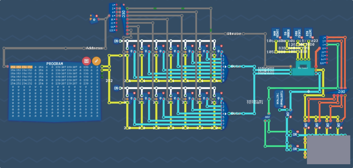
On the left, we have a bit of programmable memory which I’ve programmed with our brick texture, in the middle is that bundling block that bundles up tiles over 8 ticks that I showed off earlier. It’s perfect you see, because the driver takes up to 8 ticks to finish drawing, so taking 8 ticks to load the next tile isn’t a big deal.

Over on the right we have our driver and screen and– wait a second… that driver chip is looking pretty gross. Turns out that in this game, a chip only has a cyan square if the corresponding grid-square inside the chip also has some kind of chip in it, and wires don’t count. If you were curious as to why the outputs of the control chip were spread so far apart, this is the reason why. You can only have one pin on each individual grid square. Anyways, I added a few constant OFFs to the empty squares to fill in the gaps, so that’ll look neater in the next screenshot promise.
Anyways, lets see what this looks like!
Well that doesn’t look right… And sure enough, stepping through the individual ticks shows that my error was that I had wired this part backwards, so it was in fact drawing the screens right to left instead of left to right.
Anyways, I fixed that now, lets step through the ticks and we can see what the chip is actually up to.
Just while I’m testing the graphics driver chip, I logical ORd $0100 0000 0000 0000 into the data line, as that’s required to make the screens actually update, otherwise I’d have to strobe everything at once with just that constant above to update everything at once. I suppose it’s some sort of v-sync.
Ooh, this looks promising. 4 ticks, 4 outputs. Seems to work pretty well! Does it do the rest of the row?

Looks like it does.
But hold on something looks wrong.
Did you go back and have a look at the circuits to spot the bug I intentionally left in? (genuinely did have this the first time around, here’s the proof lmao)
Everything looks weirdly blue. Shouldn’t these bricks be yellow and orange? And honestly, the answer is yes.
The issue is coming from inside the driver, essentially the 3 byte colour input is being truncated to 2 bytes before it gets output again, beacuse I ended up using 16 bit switches instead of 32 bit switches in the circuit that decides which colour to output.
After switching the switches to the right switches, we can now run our code again and see that it’s working as intended!
Anyways, thats the end of this part of the story.
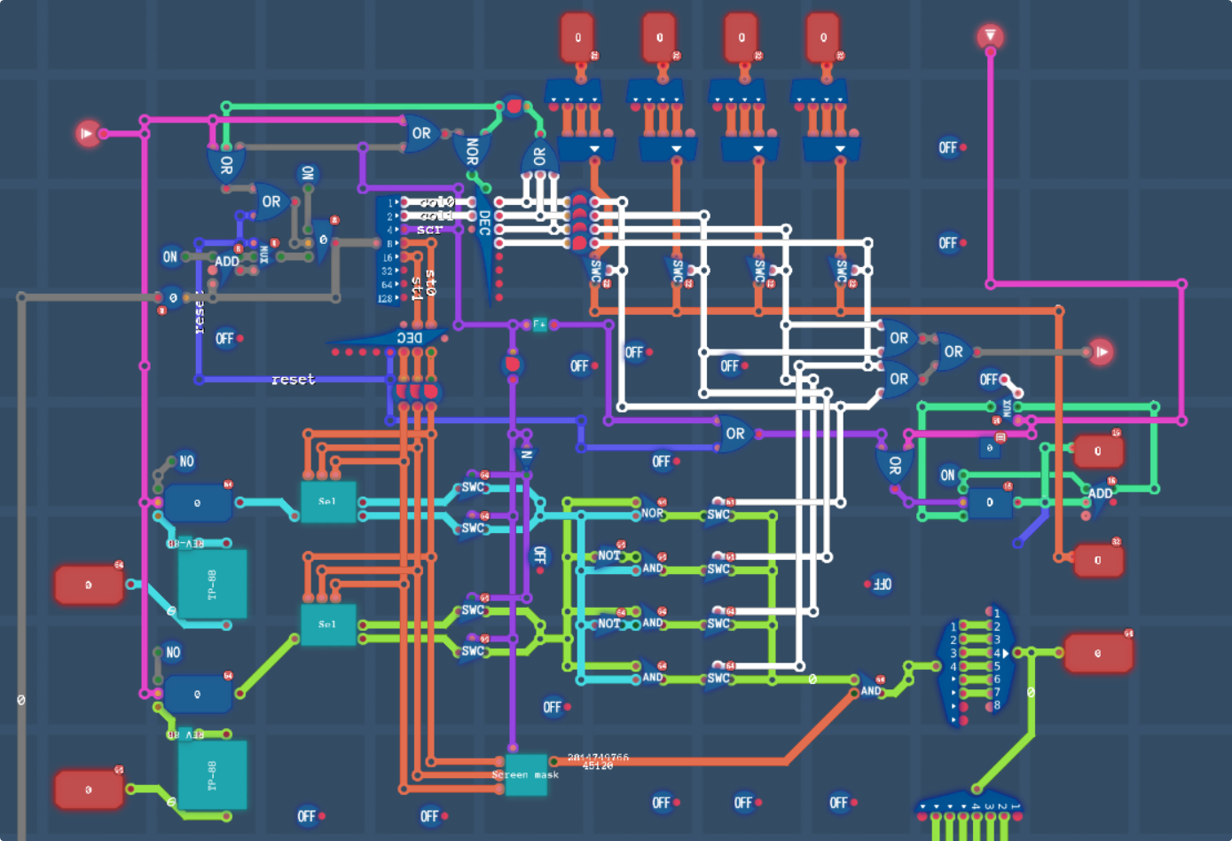
Actually wait, I did say I’d show you the mess that was my own version of this chip, not just one that I put together to explain my thought process and journey just for this blog. I’m sorry if it’s hard to see and understand what’s going on. fundamentally it’s the same as the chip I built here, just with most of the internals strewn about the place instead of packaged away inside tidy little chips.
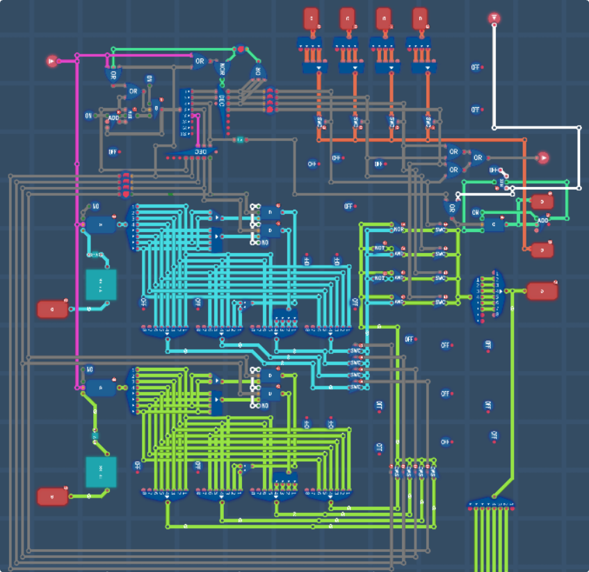
Broadly, black is my control lines, they cover both colours at the top, and screens down the side. Blue is bitplane 0, green is bitplane 1, and orange is the colour inputs. You can see the clock in the top left and the screen counter on the right. There is also a bundle of green lines going towards the bottom, those were to help me with debugging.
Each of the lines ran to a column of wire probes, which I then used to inspect what was going on inside the chip from the outside (wire probes in a grid square replace the cyan square with either a red or green circle.)
Anyways. Thats enough of that, let me tell you about the one massive bug I encountered that made me have to rethink everything.
The One Massive Bug I Encountered That Made Me Have to Rethink Everything
Have a think about it, the way that I implemented drawing to screens leaves a pretty big issue, right? Please tell me that it actually isn’t this obvious and I’m not dumb for missing it…
Ideally I want to be able to draw each tile in a certain palette right? Thats what makes tile based graphics compress really well, yknow.
Well uhhh, the way that this chip works makes this whole paradigm fall apart. Let me explain
On the first strobe, we latch the first tile and the first tile’s colours, right?
Then on the second strobe, we latch the second tile and the second tile’s colours.
BUT
but we still havent actually finished drawing the first tile yet!!!
That means that when we go to draw the rest of the first tile, it’ll have the colour palette of the second tile. Thats kinda a big problem.
Okay so what to do about this. uhhhhh
shit
Alright so, heres the solution. If a screen has 2 tiles on it, we have to write it twice now. Or phrased differently, we now have to write each tile to 2 screens, meaning each tile is going to take 8 ticks to draw. Let’s head back to the drawing board.
Graphics Driver, Second Revision
Outside of our screen selector chip and our control chip, almost everything we have is stuff we can reuse, nice! That saves us a lot of work rewiring our stuff, and just means we have to instead tweak how we do our drawing.
Firstly, we’ll have to change some pins between our control and our selection chips. We no longer care about dealing stuff out in terms of screens, we now have to do things in terms of tiles, which means that our control chip instead of saying what screen we’re drawing now needs to say what tile we’re drawing, and what screen within that tile. That’ll be how the selection circuit decides which tiles to draw. On the plus side though, this means no more dealing with buffers anymore.
We’ll worry about wiring up the control chip later, lets work on the easier chip first. Man, tearing out all these wires we built felt cruel, but its to help make a better driver chip, so it has to be done.
And just like that, our screen selector now has 6 possible output states.
The 3 black pins at the top from left to right are now Tile 1, 2 and 3, rather than Screen 1, 2, 3 and 4. The pink pin is our screen selector, either the first screen of a tile, or the second.
The main ramifications this has now for our control circuit is two fold. First, we no longer need to do 4 writes per strobe with some extra at the end, we always need to always do 8 writes, and two, we no longer increase the screen index every 4 cycles. The first problem can be solved by allocating bit 2 of our counter towards the drawing part of the circuit, leaving bits 3 and 4 to be our strobe counter. The second challenge requires a little bit more finesse.
Here are the main differences.
- Our tile counter is now on bits 3 and 4, and a new screen flag is on bit 2, which is both sent to the output, and replacing the 4th screen override on the counter continue. This is because we always want to draw 2 screens per tile instead of one.
- The tile decoder no longer resets on its 5th pin, but rather its 4th. This is because we now need to reset after completing 3 draw cycles, as a draw cycle is now an entire tile at once, rather than just one screen.
- The screen counter now updates either when the tile counter reaches 4 (indicating we have completed a 3 tile set and must advance to the start of the next 4 screen block) or when the screen bit goes from 0 to 1. Remember when I said I had rising and falling edge detectors, this is why.
Everything else can stay the same.
Hmm, what happened here? Something went wrong…
Stepping through the code, we can see two things.
First some kind of race condition is happening, which in the short term can be solved by strobing less often, but in the longer term is gonna take a bunch of work to sort out that I haven’t actually done yet.
Second, if we step through the drawing algorithm (or even from the screenshot you might be able to see it in the top row) when the second tile is drawing, it’s “squashing” the first one. Our output chips always output one of the colours for every pixel, so changing what our inputs are for each screen doesn’t really help us, if all the zeroed out bits from the screen selection will be set to colour 0 anyway.
We have two options to fix this. Firstly, we could either implement some kind of masking circuit to zero out any bits we don’t want to update, or alternatively, we can do our bitplane logic on the tiles first, and then perform the selection after. This second way is much more convenient, so lets do that.
And a bit of rewiring later:
“B4” and “4B” are just my custom nibble un/packers. Theyre identical to the 8-bit packers, but only use the lowest 4 bits. Here I’m just using them to condense 4 wires into a single cable.
As you can see, we’ve almost fixed our wall texture. All its struggling with now is getting the last tile out. The easy fix would be to change the strobing frequency to 9 ticks instead of 8, but that would slow down the whole PPU that we want to slot this thing into, so we need to figure out what’s wrong with it and fix it.
And I think I’ve found it? Our control circuit resets when the clock hits 24, which you’d think is what you have to do, since it needs to draw 24 times to the screen, but the issue lays in the fact that it takes a cycle for the clock to update, so when the 5th strobe happens, the clock has only hit 7, not 8, and is therefore not in a waiting state? I think? Let me see what happens when I change it to reset on 23 instead of 24…
Nope, that just makes it forget to output the colour on 24.
I’ll have to debug this when I get more time tomorrow, or if you spot something, please please let me know. For now though, I want to get this post out tonight. Rest assured, once I figure out the cause of this bug, I’ll absolutely be using this chip in my PPU, as it is a lot nicer to debug than my existing chip.
Oh yeah, let me share that for you. Its basically the same logic we went through today, but more spread out, and I decided to go the masking route, instead of selecting after pairing. Thats one of the main reasons I’ll use this chip in my PPU later.
So What Next?
Well thats simple, I want to build a PPU. I want a chip that can store a set of tiles, a set of palettes and a character map, and outputs a 32×16 screen array (24×16 tiles.) I’ve already made a start, so if you decide to read that Twitter thread I linked above, spoilers for what my next post will be about. But until then, hopefully this is enough to pique your interest, and if not, thanks for reading 6000 words of rambling about cirtuits.
Oh and while I said I’ve spent 14 hours on this project so far, writing this post has bumped that total up to 20 so uhhhhhhhhhh.
Leave a Reply to Click here for part two. Cancel reply