Fixing the Graphics Display Driver
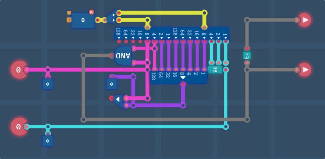
At the end of my last post, I was left with an issue. Let me quickly recap, we have ourselves a graphics driver chip that can drive 8×6 Dot Matrix Displays (screens,) but where I left off last time, we had a bug where if we stream a tile every 8 ticks, it was losing the second tile of each triad. After some investigation and debugging, I think I figured out where the issue was. Lets look inside our controller chip inside the driver.
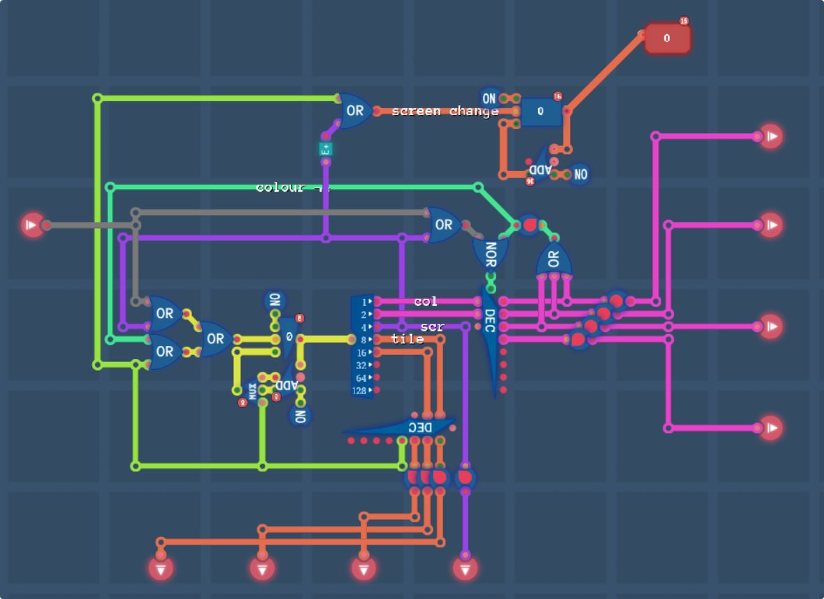
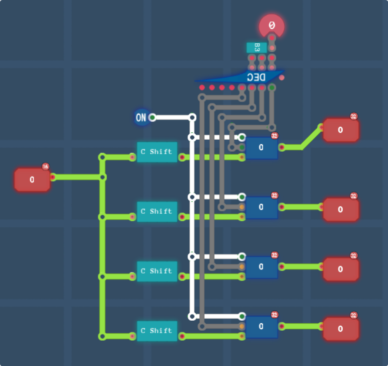
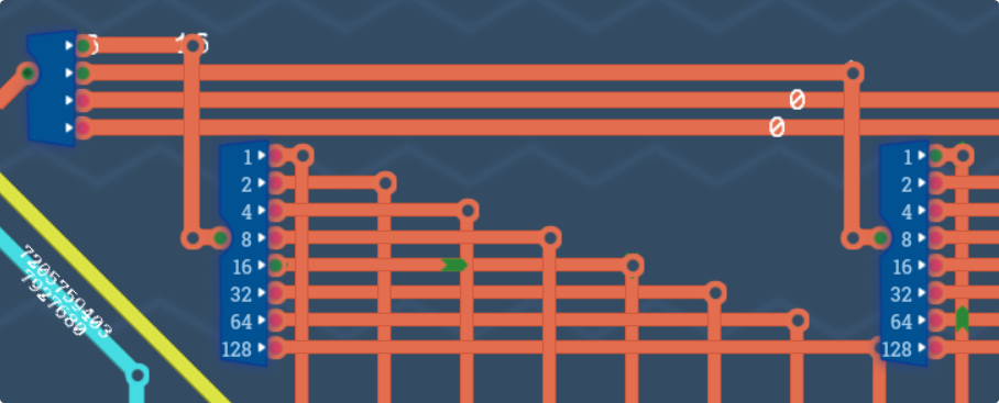
The register just to the left of the center is our cycle counter. This controls which tile, screen, and colour we need to draw, and when it hits 24, we reset it. The way we reset it is by switching a multiplexer from the adder’s output to the adder’s carry output, which in our case is always going to be zero. We use the 4th pin of the decoder as an implicit equality test, as 24 is #0001 0000, our decoder is hooked into bits 3 and 4, so this would be #10, or the 4th pin.
This means that when the counter hits 24, the next cycle is guarenteed to put the counter back at 0.
This is where the issue lies. The counter has a 1 tick delay between inputting the data and outputting it. While it reads a new value on one tick, its still outputting the old value until the next tick. This causes us a problem when we strobe on this rollover tick, as the strobe will coincide with the counter chip rolling over, and we end up double-counting our 0 tick. This means that when the fifth strobe comes through, our counter is stuck at 7 instead of waiting at 8 for a new strobe.
The solution that I’ve found is kinda simple, when we do our roll over tick, we should instead switch the counter to the value of the strobe line. If the strobe is low, it can return to 0 and sleep as normal, but if the strobe is high, it should go straight to 1. This is because our outputs are alreaady delayed by a tick, and #0001 0000 is almost the same as #0000 0000 in terms of the colour and screen selector.
So lets make this change and see what the output looks like.
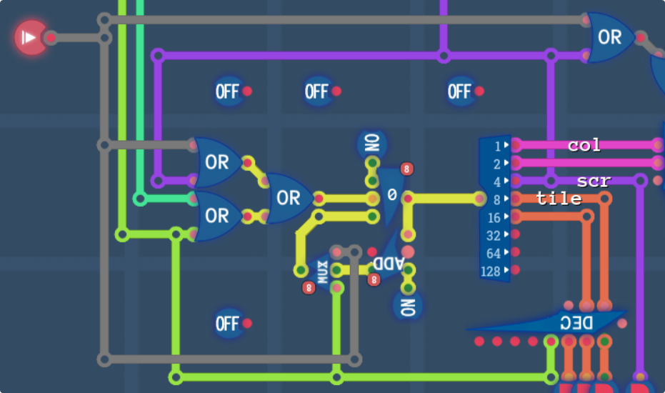
All we’ve done here is run the strobe line into the multiplexer instead of the carry constant 0. And now lets see what this does.
Almost got it. If you have a keen eye, you’ll notice that the bottom right screen seems to have the wrong grey, and you’d be right. The grey on the bottom left screen is the uninitialised default colour. That means that the first colour of the first screen of the 4th tile isnt drawing, and I can already see why that is. When we tick over to 24, we’re relying on the fact that $10 is about equal to $00, but that isn’t entirely the case. The tile counter is still looking at the 4th tile on that tick, not at the 1st tile. We should be able to patch this quite easily though, by treating the 4th and 1st tile the same, just like this.

Now lets see if this has fixed our problem.
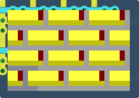
It looks beautiful!
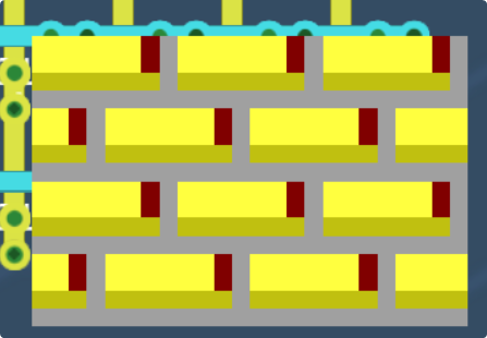
One last thing to test, whether our colours are working as expected. Let me quickly monkey patch something to our testing rig to change the colours every tile. I just hooked the strobe line up to a toggle latch that enables/disables XORing the colour by 128 blue, just anything so that we can see the colours change per tile.

And just like that we’ve done it. We have a graphics driver that can take a stream 8×8 of tiles and output them to the screen. It keeps count of where it is on the screen so that it doesn’t overwrite itself, it can handle multiple different palettes on a single screen, and it can continuously write if it recieves a strobe every 8 ticks without running into race conditions.
Picture Processing Unit Design
Now I’m going to be honest, I don’t really know much about how to make a picture processing unit other than the high level stuff you can learn watching Retro Game Mechanics Explained, I kinda know what I sorta need it to do, but I’m by no means an authority. But lets face the facts, I’m making a PPU for fun, not trying to implement any specific control mechanism, and also my display medium is an array of 8×6 screens, not a CRT monitor, so I’m going to take some creative liberty on this one.
First up, lets talk broadly about what we want our PPU to do.
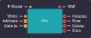
- It needs some access to memory. Either we can run IO pins to an external memory chip, or we can try and embed some video ram into the chip itself. While it would make the chip smaller to offboard the memory, we are very much racing to get as much data as we can into our driver, as ideally we want to be pumping tiles into the driver as fast as it can accept them.
- It needs a method to write to that memory, but we also must consider that the PPU will have to read from that memory at the same time, so we can only issue write commands when the PPU isn’t currently reading, and by extension isn’t drawing to the screen.
- It needs a Forced Blanking (F-blank) signal. This is how the CPU can tell the PPU that it intends to write to memory.
- It needs some time between frames that the CPU can use to write to memory without interupting the drawing process. It’s all well and good having a F-blank toggle, but if it’s going to leave artifacts on the screen, it’ll cause us problems down the line.
- It’ll need a way to tell the CPU that it is done drawing for the frame and is going to go to sleep to allow the CPU to update the data. The SNES uses a strobe signal called a “Non Maskable Interrupt” or NMI to achieve this, and that signal is sent the moment that Vertical Blanking (V-blank) starts.
- And lastly, it needs a way to take the output from our driver chip and convert that into screen outputs. Most of the logic here will have to be built into the screen, but the least we can do is unpack a screen number into a row and column number to simplify external logic.
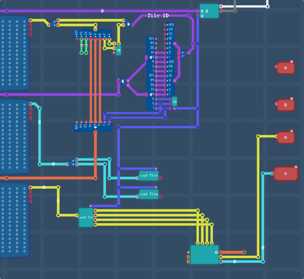
Lets get the pins onto a component board so that we can see what we have to work with.
Apologies for the low quality screenshot, the game doesn’t like drawing large chips in the preview.
In terms of the actual specs, for our hypothetical PPU, lets start with just 1 background layer which consists of 24×16 2BPP tiles. I’ll explain why below. I’m fully aware that 1 background layer and no sprites doesn’t make for the strongest PPU in the world, but right now we’re just developing a proof of concept. Once we know what we’re doing, we’d theoretically be able to expand it. That being said, I don’t have it in me right now to expand it, so that’ll be a project for future me. It’s not like the game’s simulation is going to be able to handle how far we’d want to push it to expand this though anyway, so c’est la vie.
The Maths Zone, Part 1
We already know by how our driver works that we can draw 1 tile every 8 ticks. In our final PPU, we need to fill a 24×16 tile (or 32×16 screen) array. This equates to 384 tiles. That’s gonna be a magic number btw, so lets remember it. 384.
If we convert that drawing time into ticks, we get 3072 ticks per frame.
The game simulates at about 10 kHz, which means that if we didn’t include any down-time for V-blank, then we’d be able to achieve 3 frames per second. If we allowed our PPU to have 1024 ticks of down-time during V-blank, we’d have 1024 ticks to write memory, and 4096 ticks per frame.
Let me explain why I decided to make our screen 24 tiles wide and 16 tiles tall. The simple reason is that this would make the total size of our screen 32 screen modules wide, and 16 screen modules tall, and leave us with 512 screen modules total. All three of these numbers are powers of two. This means two things for us: we don’t have to do any maths to choose our row and column, and we don’t have to worry about implementing any kind of reset into our graphics driver, as we can just let the screen number overflow 9 bits and not care about it.
Lets think about timing and memory next.
Each character consists of 2 bytes of character data, 16 bytes of tile data, and 2 bytes of colour data, where we can format our colours as #0RRR RRGG GGGB BBBB, bitshift each colour channel up by 3 bits to get a colour. This wouldn’t allow us to get a perfect white without extra logic, but we can implement that if we decide we want it.
This equates to needing to pull out 20 bytes of data every 8 ticks. If we use a single memory module, or an external memory bus, we simply wouldn’t be able to pull enough data for our graphics driver fast enough. This is why we’re going to be using onboard memory.
Onboard Memory Chips
We’re going to need to store 3 types of data for our PPU to work.
First off is the “Character” data. A character is a block that defines how to draw a specific tile to the screen. This is 2 bytes wide, and consists of a Tile ID, a colour palette ID, and some extra flags we can define. Lets follow the lead of the SNES and make our character format be #PHVC CCTT TTTT TTTT. T will be the ID of our tile, C will be the palette number from 0 to 7, H will let us flip our tile horizontally, and V will let us flip our tile vertically, and as we have no drawing logic in place about how to draw tiles to the screen yet, lets not worry about the P bit and let that always be 0.
We’re going to need 768 bytes of memory to store our 384 characters.
Next is the “Tile” data. This is the 2bpp graphics that get loaded into the driver chip and drawn out to the screen. As our memory modules can output data onto 16 bit lines, There are 3 ways of defining our graphics data.
- The niave approach: Each pixel of a tile is two bits, each byte therefore is 4 bits.
- The niave but useable approach: We put all the bytes of the first bitplane together, and all the bytes of the second bitplane together.
- The one we’re going to use: We interleave each row of each bitplane, so address 0 and 1 will be the top row of both bitplanes, address 2 and 3 will be the second row, and so on.
Why are we doing this? Well, we can make our RAM chip have a data width of 16 bytes. This means that sending the address of 0 to the RAM chip will get us the first 2 bytes, address 1 gets us the next two bytes, and so on. We can then unpack the two bytes and pass them into our little bundling construct that we designed yesterday for our testing machine.
If our tile IDs are 10 bits wide, we’re going to have to have space for 1024 tiles, and at 16 bytes per tile, that means the tile memory chip is going to need to be 16,384 bytes wide, and contain 8192 memory addresses which is a full 13 bits of the address input.
Lastly, we’re going to need our Colour Graphic RAM. This will be the smallest of our ram chips, as we only need to worry about having 8 palettes, each with 4 colours. If we decide to do any of the enhancements at the bottom of this post, we may find a reason to expand it (e.g. 3bpp graphics would require palettes of 8 colours, or having two layers would allow us to have seperate palettes per layer. If we decide we want to try and draw out sprites onto our screen, we’ll need palettes for sprites too.)
8 palettes x 4 colours x 2 bytes per colour = 64 bytes. (For reference, the SNES’s CGRAM has space for 256 individual colours on it’s palette, we’re only using 32.)
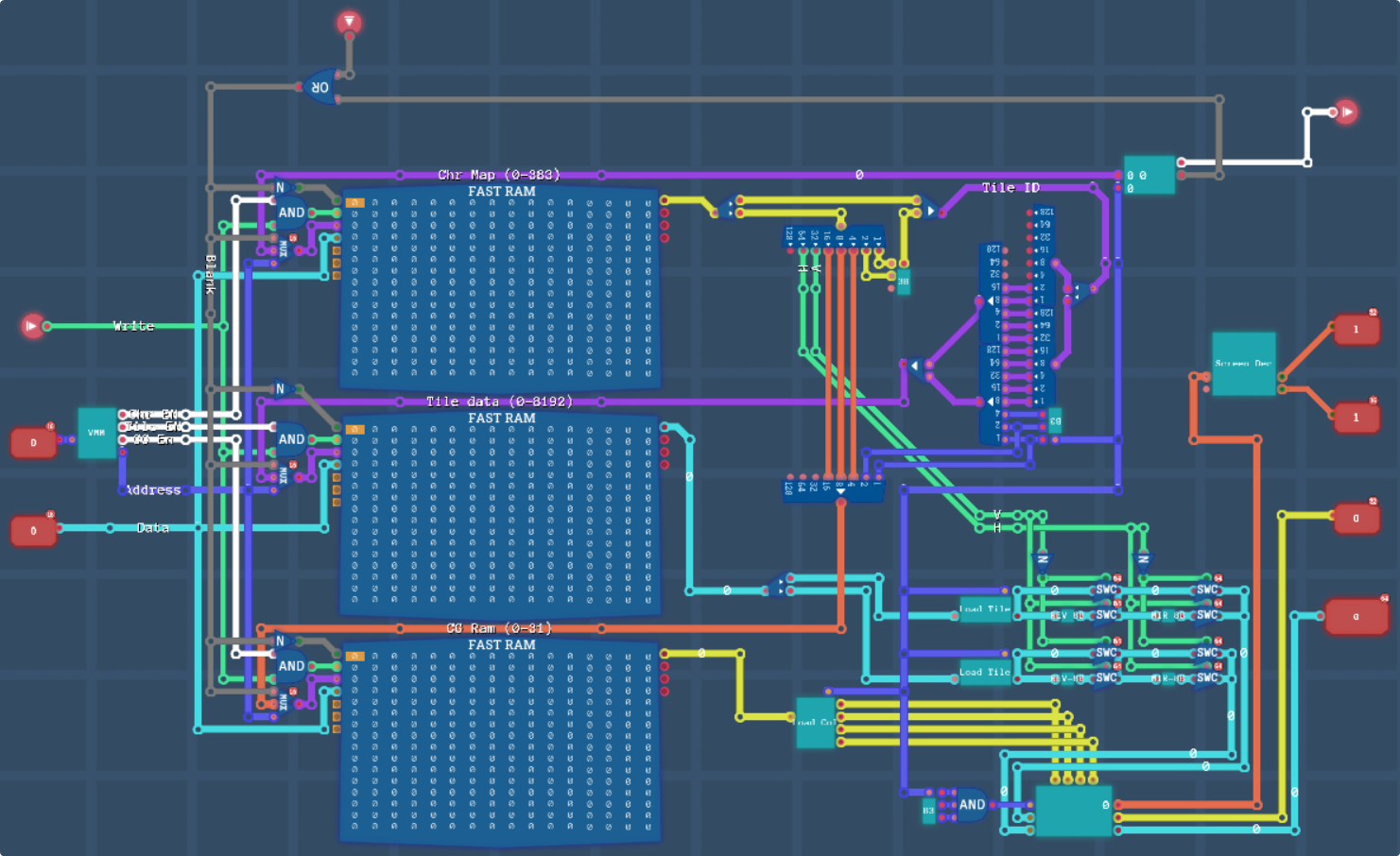
Let’s get some memory into our chip.
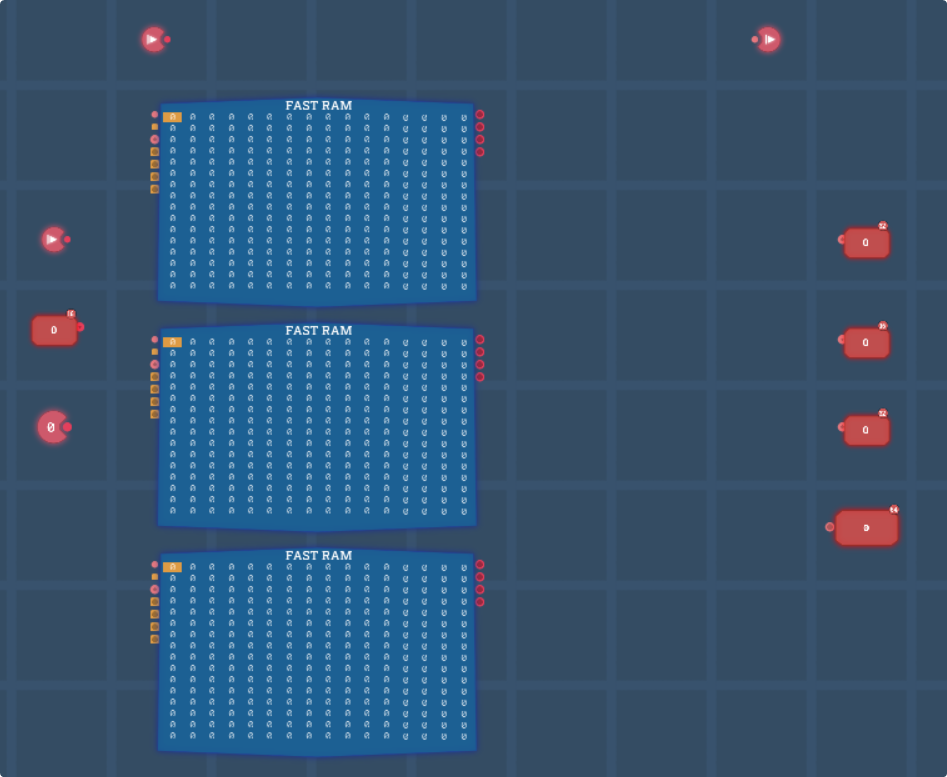
Good grief, memory chips are big… I’ll probably leave them exposed though and just make our PPU chip bigger.
Let me quickly just set all these to 16 bits, and configure their size as well.

Oof, 16kB of ram is expensive, who’d have thought…
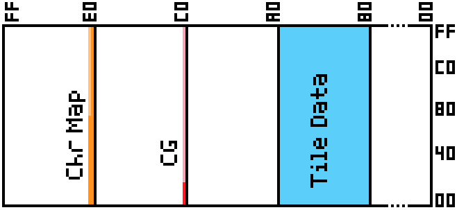
From top to bottom, we have our character map, our tile data, and our CG data.
Let’s Figure Out What to Do Here
We already know roughly what we have to do. We need to allow writing to the memory during a blanking period, we need to read from the memory during a draw cycle, fetch and prepare the tiles, and then pass those to our driver. Then just before we output to the screen, we need to calculate the row and column.
I’ll do each step individually so that we can try and compartmentalise stuff as much as we can.
But first a little bit of information on the pinning of a RAM chip. On the left of a ram chip are 4 inputs: Read, Write, Address and Data. On the right is 1 output: Data. When the read pin is high, the RAM chip will output whatever data is being stored at Address onto its output Data pin. This is an instant action assuming the data has not changed. Just like with registers, if the data at the address changes, it’ll take a tick to propogate (the clock module even explicitly states this, by saying “Data is read during the first half of a tick, and written during the second half.”)
If the Write pin is high, then the data on the Data input line will be written to the address specified by the Address pin. This chip is essentially a massive array of 8 bit buffers with a selector pin saying which one to interract with.
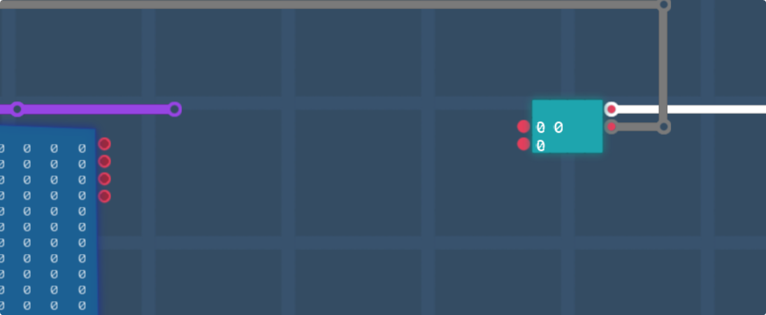
In the screenshots, you’ll see 4 pins on each side for the data input:
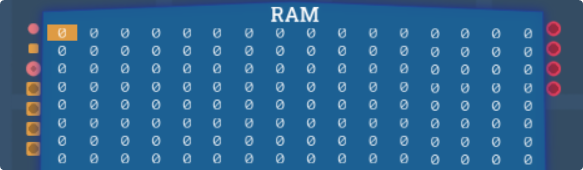
This is almost exclusively used in the absolutely bonkers usecase where you need your ram to have a data width of 128 or 256 bits. In these cases, the 3 auxillery data pins let you run 3 additional 64 bit lines into and out of the chip. For all other data widths, only the topmost data pin on each side is used, the rest can be ignored.
Writing Data to the PPU
When the F-blank line is high, we need to do two things: First we need to disable reading from the memory. This won’t explicitly halt the drawing algorithm from happening, but it will “blank” any screens that try to be drawn during F-blank. We’ll also need to switch the address pin to being controlled by the input address, rather than the chip’s internal circuitry. With this in mind, lets have a look at the inputs for one of our ram chips then.
Now, there is a lot going on here, 6 different wire colours, so lets go through them one by one.
- The outermost blue wire is Data. This is connected directly to the Data In pin of the PPU.
- The next black wire is our F-blank signal. When F-blank is low, we need read to be held high, and when F-blank is high, we need to switch the address inputs.
- The third teal wire is the Write signal. This is wired directly to the Write pin of the PPU.
- The fourth white wire is a selection line. We’ll go over this in a second.
- The fifth blue wire is the input address, though we’ll have to do some work to it before passing it to the ram. Again I’ll explain later.
- The last purple wire is the internal address. This is going to be controlled by the PPU itself, and is how the chip can retrieve data to feed into the driver.
We have this same construction for all three of our ram chips. We can’t just wire the purple lines together, as we’ll need to address different tiles and colours at the same time, whereas for writing to the chip RAM, we can only use one address line anyway.
Now let’s talk about the address space of our chip.
Each of our ram chips is addressed from $0000. The character map goes from $0000 to &0180, the tile data from $0000 to $2000, and the colour data goes from $0000 to $0020. This is a problem, as we only have one input address to work with. This means we’re going to have to specify a memory mapping to both dictate what addresses correspond to each RAM chip, and also convert the address from a board wide Bus address into a local offset for the chip.
So lets do some memory mapping.
In terms of the data, we’re gonna need at least 13 pins for the tile data alone, so that leaves us with 3 extra pins to work with for our character and colour data, as well as any other stuff we’re gonna want to put on this chip in future, which I’ll discuss at the bottom of this post. Just because we don’t need that much memory (yet), I’ll build our chip to only use the top half of the system address space, though if need be, we can just edit our memory mapper to change how things are fed into this chip. If we really wanted to we could give this chip only 14 pins for addressing instead of 16, though in Turing Complete, both would be a 16 bit input anyway, so oh well.
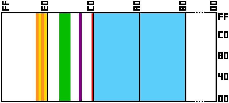
This chart is drawn to scale. Each column is a page of 256 bytes. Each pixel represents 4 bytes (I didn’t want to draw this diagram 256 pixels tall.)
I’ll drop this graphic down in the improvements section as well so that we can see what sort of things we could do with this extra space, things such as having a larger screen requiring a bigger character list (4 orange columns instead of two), more colour options, Object Attribute Memory, Sprites, 3 or 4BPP graphics, all sort of extra bits and pieces.
The big blue chunk on pages $80 to $9F will be our tile data. The orange chunk on pages $E0 and $E1 will be our character map, though we don’t need the last quarter of it, we’ll map it anyway and trust that it won’t be used. Page $C0 will be our palette. I’ve mostly mapped things this way to make building the memory mapper easier, though if we need to shuffle things around, we can tweak the memory mapper as needed.
And lastly, you may have noticed that all our addresses are in the top half of the address space. This is so that if we decide to use this PPU on the same bus as a CPU, we can use the 15th bit of the address line as a toggle switch between CPU space and PPU space. If we decide to build our PPU onto a dedicated PPU space address line, (e.g. the A/B Busses for CPU/PPU space in the SNES) then we can ignore this detail.
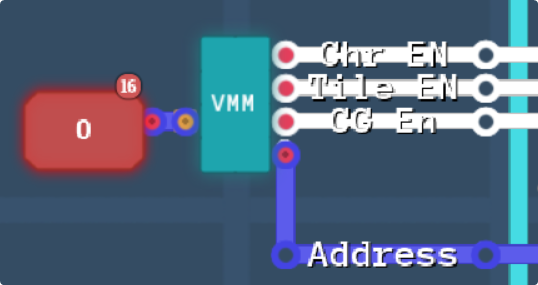
This VMM will be in charge of converting the Address bus input into local memory addresses, and also deciding which of the 3 chip’s Write signals to enable. Lets get that wired up.
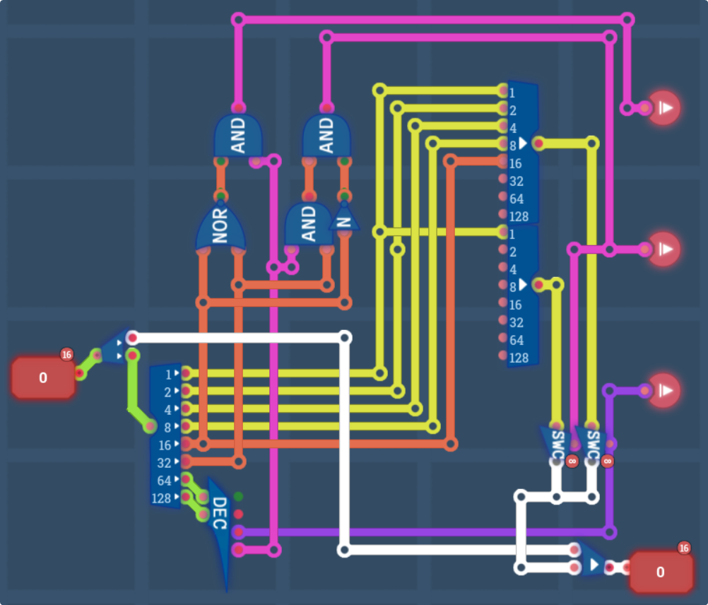
Now, this chip isn’t exactly perfectly robust and mapped exactly how we want it to, but for the time being, this will do for us. As long as we arent trying to write to out-of-bounds memory addresses, we’ll be fine. Data only gets written when write goes high anyway, so we don’t need to worry about it. The logic in the top left is a test for ¬(B1.4+B1.5) and ¬B1.4+B1.5, both then ANDed with B1.6*B1.7. This tests that we’re somewhere between page $C0 and $CF, and between page $E0 and $EF respectively, which are used for our CG and character addresses.
At the bottom is a decoder, essentially testing which quadrant we’re on, $00-$3F and $40-$7F are both disconnected, as we only use the upper half of the memory space. $80-$BF are wired directly into the chip enable for the tile data. $C0-$FF is used in the logic above to enable one of the other chips. And on the right, we have some wires for deciding which bits of the top byte of the address should be passed through. For the tile data, its the bottom 5 bits, for the character data, it’s just the bottom one bit, as we only need 2 pages of memory, and for colours, we just want one page, so we don’t output anything on the top byte.
Lets see what our memory space looks like now.
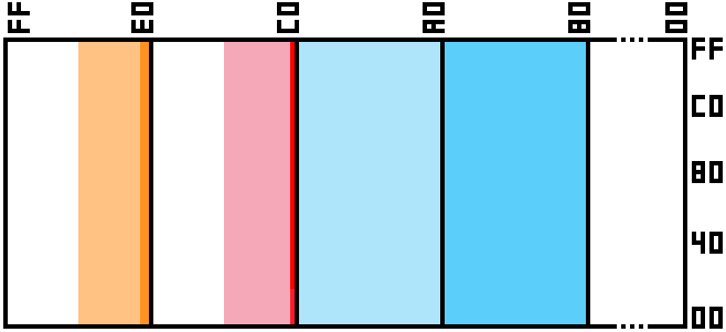
Huh, thats interesting, It’s filled up a lot more than we expected. That makes sense actually, this behaviour is called “mirroring.”
For example, our tile data is set to be anywhere where B1.6 is low and B1.7 is high, corresponding to pages $80-$BF, but then when we went to map the input addresses to output addresses, we never connected B1.5 to anything. This means that it doesn’t matter what B1.5 is, we’ll still go to the tilemap chip, and we’ll still be writing to the address as if B1.5 is 0. In essence, writing to $8000 is exactly equal to writing to $A000.
As we don’t need the memory for anything else, we can leave this behaviour as is. When we decide to add enhancements that would require we use these spaces, we can update our mapper to rebind addresses accordingly. Of course, we also need to pay attention to the size of our memory. CG RAM only uses 32 addresses out of the 256 that are linked to it, and Character RAM only has 384 addresses in it, not 512, so our PPU will still crash the simulation if we try to write to these addresses.
Anyway, thats enough for now about memory mapping and writing to the chip. None of it is useful if we can’t do anything with it.
Clock Cycles and Vertical Blanking
As we calculated earlier, it’s going to take 3072 ticks to draw the frame and then we’ll pad the clock to 4096 by adding 1024 ticks of V-blank.
We have to do four things when V-blank starts.
- Stop the drawing algorithm from continuing before it goes out of bounds.
- Strobe all the screens with $0100 0000 0000 0000 to update them.
- Send a pulse down the NMI output pin.
- Some number greater than 8 ticks after V-blank starts, we have to strobe all the screens.
For this, we’re going to need a timer, which for the most part will keep track of the V-Blank timing and drawing routine by telling the tile maker which tile it needs to get next, and which tick of the 8-tick cycle we’re on.

Interestingly, this chip only has outputs, no inputs. The two numbers will represent the cycle tick and character index. V-blank will be on during the entire duration of the V-Blank period, and we can OR this into the control line with F-Blank to disconnect internals while we don’t need them. Lets create the chip now.
This is a pretty simple chip. The bottom three bits become our tick counter from 0 to 7, leaving the next 9 bits to be our tile counter from 0 to 511. Now you may be wondering why the tile counter goes up to 511 when we only have 383 tiles, and the answer is that we’re ANDing the top two bits of the tile counter together, so when they’re both high, we know we want to “draw” “tiles” 384 to 511, aka we need to go into V-blank. The rising edge detector is there to strobe our NMI when V-blank starts. We don’t quite have our strobe line set up yet, but that will just take a simple tick delayer and can be done outside of the timer chip. Lets go and wire this baby up.
Actually, yknow what might be a bit more useful here, something to wire it to.
Fetching and Parsing Characters, Colours and Tiles.
Lets start off simple. First we need to fetch the character from our table. This is just going to be the tile index and nothing else.
If we remember, our characters are in the format #PHVC CCTT TTTT TTTT. This means our tile ID is the whole low byte, plus 2 more bits, the colour is the next 3 bits, and the flip bits can be handled seperately.
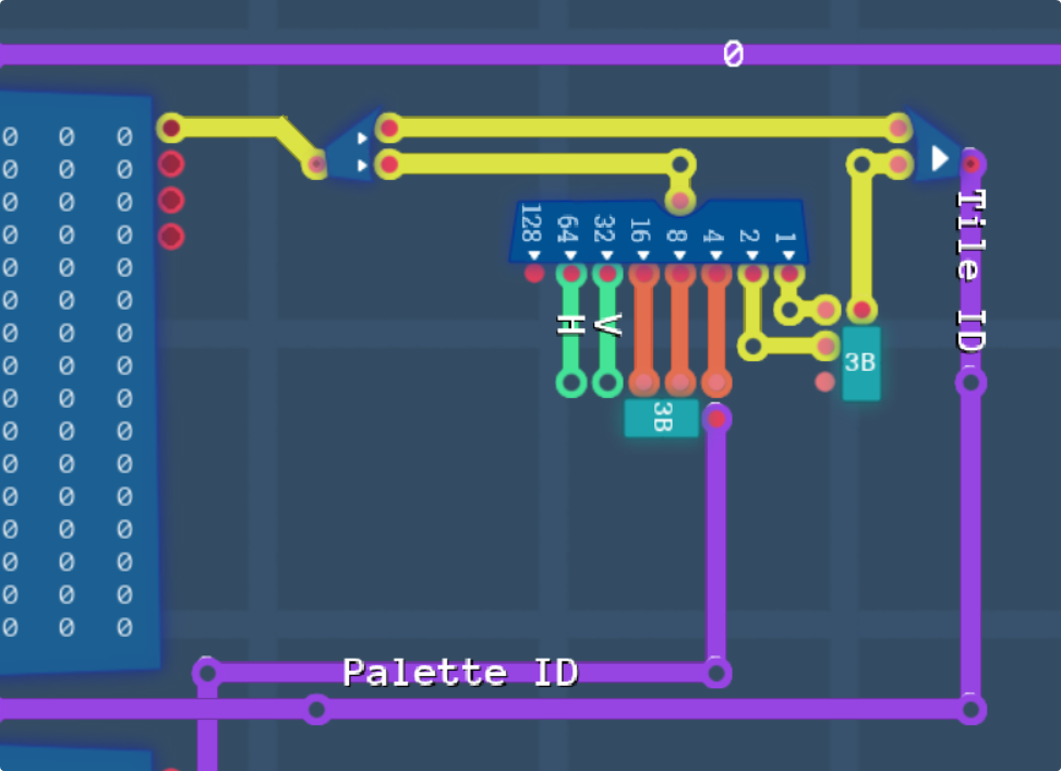
You may be wondering whats stopping this from just loading an invalid address when the clock ticks onto tile 384, and the answer is that the moment the clock goes to 384, V-blank enables, and that switches the address of the RAM to the external address bus, not to the clock’s tile counter. Anyways, now that we know what tile and palette to use, we can set these up too. I’ll build the tile chip just based on the circuit we had outside on our little computer, so if you want to know whats going on there, go read the previous post.
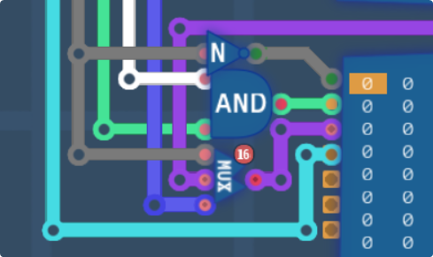
As for the colours, we need to load 4 values and do a little bit of bit-shifting on each one to get the colours that we’ll have to pass to the drawing chip. First things first, lets make a little utility chip to convert our #0RRR RRGG GGGB BBBB into $00RR GGBB.
I do enjoy a nice 0-cost chip to play around with. Time to use this to decode our palette to read into the driver.
A very simple chip. Waits for ticks 0 through 3 to latch buffers 0 through 3, and just always outputs those latched values. The driver chip also latches the colours when it is strobed, so these ones being overwritten won’t cause us any problems.
Now lets start putting it all together, and here’s where the magic comes in, remember when I said at the start that we want our tile data formatted as interlaced bitplanes (like, BP0 R0, BP1 R0, BP0 R1, BP1 R1, …), it’s because the data width of our tile RAM is 16 bits. Each memory address gives us 2 bytes, and since our bytes are interlaced, it means each memory address gives us exactly 1 row from both bitplanes! We’re going to have to account for the fact we’re pulling 8 rows from ram instead of one tile, but that can be done by shifting the tile or colour index up by 3 or 2, and then ORing it with the bottom 3 or 2 bits of the tick signal from our clock.
Now I know a lot just changed, so let me try and explain my logic.
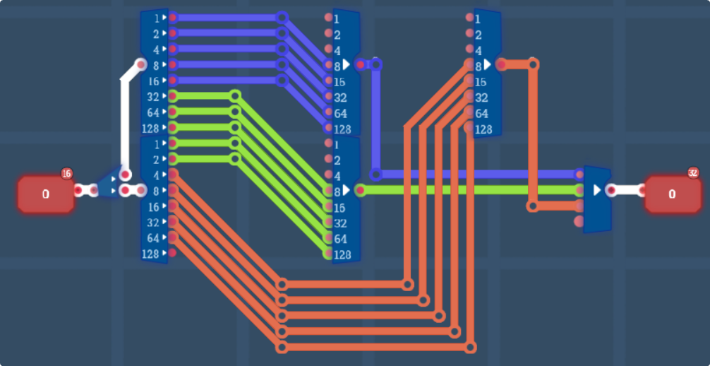
Easiest off, I wired the outputs of the two RAM chips into the tile bundler and the colour bundler we just made, as well as hooking the colours into the driver, since we don’t need to do anything else to them for now.
At the top, I rewired some stuff. Instead of packing the 3 palette bits into a single line just yet, I dragged them down and appended the bottom two bits of the tick line to it. This will allow it to read off the 4 different colour words of a palette in quick succession.
I also quickly shifted the tile ID up by 3 bits and appended the tick counter to it to allow the RAM to go through all 8 sequential rows of a tile. I’ve not connected the tile data into our graphics chip just yet, and thats because we need to build ourselves a couple of utility chips to handle the flipping of tiles. Flipping horizontally is easy, I already have the REV-8B chip that I made in the last post. Flipping each byte of a 64 bit line though isnt one I have yet. I could transpose it, reverse it, then transpose it again, but that’d take up a lot of space, so instead I’ll make a chip to reverse the bits in a byte, then have 8 of those go together to make the 64 bit version.
Not my cleanest wiring, I’ll admit.
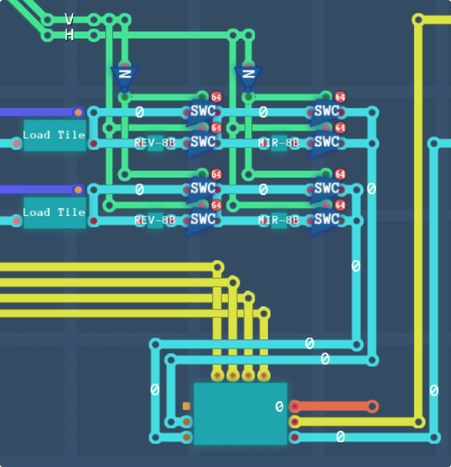
The new chip here is MIR-8B, which is just 8 REV-1B chips stacked on top of each other, in essence it takes every byte in the 64 bit line and reverses it. REV-8B still just reverses the byte order of the bytes. Reversing the byte order reverses the rows, and therefore flips vertically. Mirroring each byte of the tile mirrors it horizontally. Once we have our mirror settings, thats when we can get our bitplanes into the data chip.
Drawing The Screen
Now that we have our colours and tiles being fed into the graphics driver, there is one last piece of the puzzle. We have to strobe the driver to let it know to do it’s thing. We can do this by just ANDing the 3 bits of the tick line and strobing when that comes out high, since the 7th tick is when the final row of the tile is available.
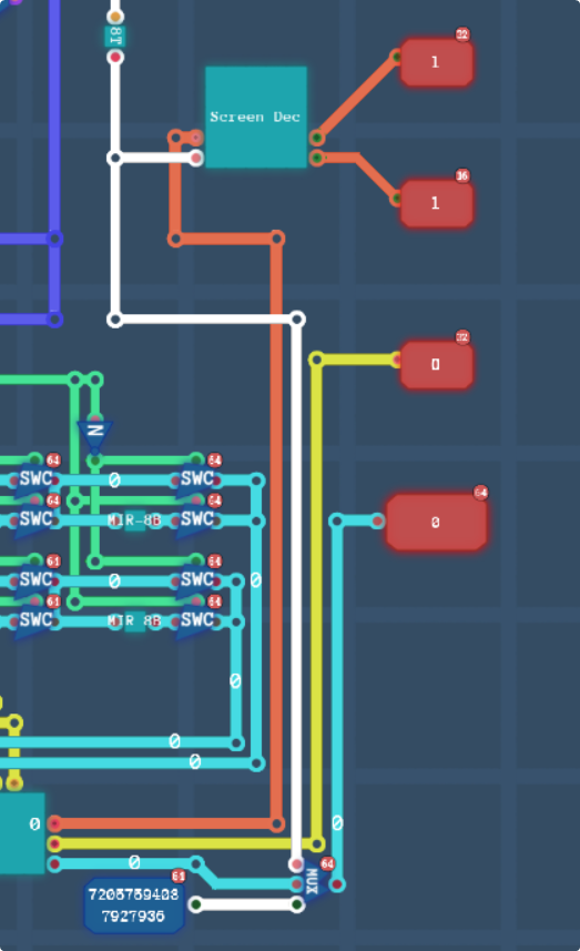
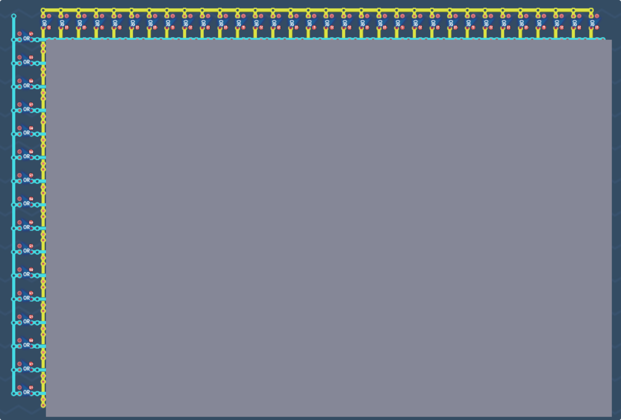
Then we need a way to tell the screen array which screen to update, so our next chip will be a screen decoder. It’ll most likely be a very simple chip, we’re just bundling it up so that we dont have too many wires floating around.
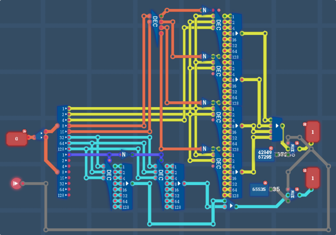
Not exactly my most graceful chip. Let me explain whats going on here. To convert a number into a single pin, you use a decoder. To decode 4 bits, you use 2 decoders, and to decode 5 bits, you use 5 decoders. But why am I using decoders here instead of just putting out numbers and leaving the rest to the screen itself. Well, you see that mux at the end, thats going to do us some magic.
The intention here isn’t that the screen array will turn on the screen matching the row and column number. The screen array is going to enable any screen where the corresponding bit of a 16 or 32 bit number is on. Theoretically this means we can update two screens at once with identical data, but we don’t need to use it for that. What we need is a way to turn on all the screens at once. Don’t forget, at the end of a “frame”, we have to send $0100 0000 0000 0000 to all the screens to force them to update. This is what will allow us to do that, and thats what the black input pin on the left controls.
It doesn’t matter that the pin is now always outputting a 1, even during blanking, because as long as the Data output line is 0, nothing is going to be written to any of the screens. I’m sure that there is a tiny amount of optimising that will help the simulation if I add a switch to the row and column selector to only draw when the driver is drawing, but we don’t care about that.
You may have also noticed that we have nothing on the GPU or in the graphics driver that resets the screen number. In our particular case, where the screen size is a power of two in both directions, we don’t care about overflow, because $00-$1FF is mirrored by $200-$2FF. Same concept as the memory stuff above yknow. Disconnected pins are always 0, regardless of what the input wants them to be.
And we’re almost done!
Just one last thing, one last unconnected pin that we’ll have to wire up to something. Remember how I said we need to wait about 8 ticks after V-Blank starts in order to strobe all our screens at once, this is the time that we implement that.

This feels unreasonably scuffed, oh well, it’ll get the job done. 8 ticks of delay from the NMI to allow the driver to finish pushing tile data, and then we can flush all the screens at once.
Moment of Truth. Does It Work?
Truth be told, it hurts tearing out the old testing rig we had going, but this is what we have to do for science.
Help my computer is already starting to lag and get hot…

Give me a second to go clean up some holes. I don’t know if more holes is good or bad tbh, more holes usually means more wiring, but fewer holes means denser logic, and I don’t know which one to be more scared of.
Hmm…
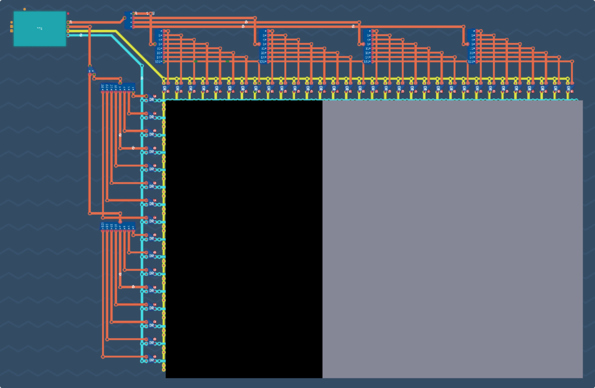
Why did only 12 columns light up? That’s not good… Gosh where do I even start looking for the source of a bug like this… I guess a good starting point would be to OR $0100 0000 0000 0000 into the data line to see the updates happening in real time.
Thats odd, only one column is meant to be on at a time, why is it outputting both columns 5 and 0. Let me go take a look at the row decoder chip. Oh good grief I missed some wires! Wait, was that in the screenshot above? Yes it was, good grief, I’m a bit of a sausage aren’t I. Let me fix that and try again. Also forgot to hook up the disable line to the first decoder, which is why we were seeing two screens enabled at once.
It got a bit further this time, now it only petered out after 16 screens not 32. What did I forget to wire now? Nope, it was the same issue as last post with the colours. I used a 16 bit multiplexer on a 32 bit data line. Thats gonna be an “oops” from me dawg.
Look at that!
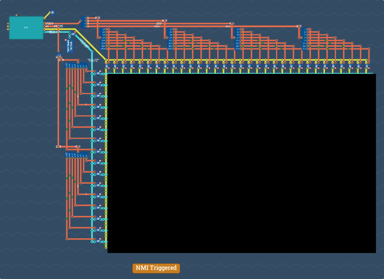
The whole screen properly initialised, and the NMI triggered for exactly 1 tick, exactly 8 ticks before the final tile was drawn. Gosh I’m so proud.
So What’s Next?
Next I’m going to build some kind of computer and program that can leverage this screen. I’ll know I’ve done something right if I can either make this thing play Bad Apple, or Doom. My next blog post will be a shorter one about building the computer. I’ll try and keep it light on spoilers, but I really really do recommend you play through this game first, it’s on steam, just waiting to be played, so please. One of the story challenges is to literally build a computer, and thats the game at its most fun if you’re doing it yourself.
You Said You’d Talk About Enhancements
I did in fact say that, so lets talk about enhancements.
Right now we have a graphics driver that can draw a stream of static tiles in order to static positions on the screen. On it’s own that’s pretty cool to be able to do, especially within the limitations of these frankly shitty screens, but if we want to do anything with this that isnt streaming videos or doubling the length of V-blank to replace every single tile every frame, we’re gonna need some more tools.
- Horizontal and Vertical Scroll Registers.
In games consoles like the SNES, the tilemap is actually 32 characters in each direction (though the screen does render almost 32×30 of them) We could add a bit of border and calculation to our PPU in order to dynamically create new tiles from the existing tilemap by accounting for horizontal and vertical offsets. Of course the primary challenge in doing this is that we’d have to load 4 tiles each cycle and then dynamically calculate which 64 of the 256 bytes need sending to the graphics driver to be drawn.
- Better quality graphics.
I’ll do some maths in a second about how far we can push this, but my best estimate is that with how slow the screen drawing algorithm is, and how little data throughput we can get from the RAM chips without making the data width utterly excessive, the best we’d be able to do is 4BPP graphics at a push, 3BPP graphics if we’re willing to cope with weird offsets, or two layers of 2BPP graphics. I don’t think we’d be able to do colour math on the two layers, beacuse drawing different colours isn’t cheap. Every additional colour to draw for a tile takes two additional ticks. That being said, if we did want better quality graphics, part of the reason I left pages $A0-$BF available in our memory mapping was so that we had space to double the tile data, which would be required to maintain 1024 different tiles if every row of a tile was 4 bytes instead of 2.
- Objects/Sprites.
Sprites while theoretically doable would have to be drawn essentially after the background(s.), mostly because an object would have to update on average 4 screens. Sometimes only two, but sometimes a whole 6 of them would have to be updated. We could add our object attribute memory (OAM) into the empty region on pages $F0-FF. Objects would need a location on the screen, like, an offset in pixels. as well as the objects’s Tile ID and other attributes. 16 pages should be more than enough to store them all, I doubt an object would take up more than 4 bytes though.
The Maths Zone, Round 2
While our simulation may only run at 10kHz, a real console would come with a 2.4MHz clock that ran its PPU. Imagine if we had that many ticks every second. Firstly we’d need to divide through by 60 to see how much of that would be in each frame, and we get 40,000 ticks. Our current PPU can draw 1 background layer at 2BPP with no scrolling in 3000 ticks. If we assume that scrolling calculations will double our time to fetch the tiles, we’d be looking at 1 background in 6000 ticks.
We’d have to subtract some time for the CPU to interract with us during V-blank, so lets say we have a limit of 32k ticks to get everything done that we want to.
And as a base line, lets assume that the slowest parts of our system is the drawing and the loading. We can load 2 bytes from tile memory every tick. All other memory loading time is more or less moot, either doable in one tick, or significantly faster than loading the tiles. Drawing takes 2 ticks per colour we want to draw, one for each of the screens we’re updating.
Lets have a look at what we can do with our 32k ticks.
- A Full Sized Screen
I don’t think we’ll be able to get a screen to display 32 tiles wide and 30 tiles tall without doing a lot of jankery to our drawing algorithms to handle the mismatched row size, but just for hypothesis sake, 32 tiles wide is 43 screens and change. Thats an awful number to work with, but not the absolute end of the world. 43 screens wide by 30 screens tall leaves us with 1290 screens to update every frame, or 960 tiles to draw. Each tile makes 8 screen updates, so that’d be 7680 ticks spent updating our one background layer.
Also it’d utterly destroy my laptop’s framerate. 512 screens is already far more than enough for it to handle thanks.
- A Second Layer
If we had a second 2BPP background layer that are just drawn sequentially on top of the existing first layer, then this will add an additional 3000 ticks to our drawing cycle. If we wanted to do some form of colour maths, this would increase the amount of ticks exponentially. 4 colours interracting with 4 colours is 16 possible colours, which means that to draw the two layers, we’d need 12k ticks.
- A 4BPP Layer
Again, 16 colours, this would take us 12k ticks to draw. Not impossible, but we wouldn’t be able to do much else. It would move the bottleneck to the drawing algorithm though. 4BPP vs 2BPP only reads twice the number of bytes, but does 4 times the amount of draw calls. Not only could we have the next two bytes prepared in that time, we could also use the extra time with a 2-output RAM chip to fetch the left, down and down left tiles in order to do screen scrolling. Same logic applies to if we were to do colour math with a second layer.
- Windowing
Adding a window would require adding a proper colour math chip to our PPU, which while a fun task, would also cause the same degree of slowdown that the rest of the ideas cause. I’d have to brush up on my colour math and window functions to fully grok how they would impact our timings, but lets assume that the absolute worst case is the half enable flag doubling the amount of colours again.
Heres where things get interesting though, if we do decide to go full ham on colour math, it may end up getting to the point where it is more efficient to write to the screens pixel by pixel rather than colour by colour. This would enable us to play around with 3 or 4 2BPP layers, or do a 2BPP/4BPP pair, etc. I’ll have to research into how to make a colour math chip.
Lets think about our screen though, 24 tiles wide by 16 tiles tall is 192×128 px, or 24.5k pixels, which would take 24.5k cycles. If we can get the data flowing in just the right way to always be drawing something, then it may be possible to go full ham on the colour math here!
- Objects
Objects naively would have to be drawn on top of the screen, using colour 0 as a transparency. But if I can figure out colour math, I should in theory be able to load the objects for a given position, and factor those into colour math too.
- H-Blank
There are some variables that need to be able to be modified between individual lines, these gaps are called Horizontal Blanking, and is the last few pixels outside the frame of the monitor. Trying to force blank and update something during H-blank will cause a whole host of problems with timing, as you’ll almost always leave a black streak visible. The SNES though for instance has a way of modifying PPU variables during H-blank called “H-blank Direct Memory Access”, which is essentially a way to change a single byte of memory in PPU space on a specific scan line. This could be implemented by storing various HDMA tables in our chip somewhere and executing those writes to memory every time the row completes. It’d require adding some form of gap to the timing circuit that could dramatically increase the complexity, but since we aren’t racing a scanning electron beam in this case, we’d be able to pull this all off in as much or as little time as we need.
So What Could Our Memory Look Like If We Did This?
If we take into account needing more memory to hold larger tiles, as well as needing more character maps for the rest of the layer data, space for our Object Attribute Memory, and some hardware mapping to various registers inside the colour math chip, here’s what we get:
Of course, not all this memory will be used, especially since our character maps are only 384 characters, not 512, and there are some new sections. Green from pages $D0-$D7 will be our Object Attribute Memory, and the purple section on pages $C8 and $C9 would be mapped to whatever hardware registers we use for colour math. We especially will need the full 32 pages for our tile data though, especially if we start doing tiles with more than 2BPP.
Can I See Your PPU Display Something?
Not yet. Maybe sometime on the weekend or next week I’ll build basic computer that can populate it with data to display, but right now I’m done writing for the day. If you made it this far and somehow didn’t read the last post, I commend you, but also go read it.
Leave a Reply