Let’s hope this is a shorter one today.
Previously on Dragon Ball Z
In the last post, I’d created a basic PPU chip. It doesn’t do much, just 1 layer of 24×16 tiles with no scrolling or transparency or other such amenities, but I kind of left it off on a cliff hanger, so today, we’re gonna build a little dedicated testing computer to slot this chip into, give it some data, and see how it handles it. If it works, I’ll be sure to publish the schematic to the Turing Complete schematic hub for anyone else who wants it to check out.
Here’s what we’re going to have to do. First I’ll have to design some tiles that I want the screen to draw. Lets start off by reusing the brick graphic that I drew in part 1, and get that tiling the screen, and then I’ll make a scene resembling 1-1 from the original Super Mario Bros, and see if we can draw something convincing.
Building A Computer
Head’s up, if you’ve not already played this game, I’d recommend doing so, as I’m going to be using a few tricks that the game intends for you to learn as part of its story while building the computer. Go play it now, no really.
First lets decide what we want/need our computer to have. Lets take a look at what instructions we want.
- A MOV instruction for moving data between registers.
- ADD and SUB for performing basic arithmetic on values and storing to a register.
- JMP, JGT and JEQ for jumping around our program.
And in terms of registers, we’ll need an accumulator for doing our math in, an address register for the PPU which ideally will increment every time we write to the PPU, and a couple of general purpose registers, and a latch that will check when the NMI has triggered to help with spinning. We’ll also need a way to indicate that we want to use an immediate value.
And just for ease of use with the PPU which is a 16 bit chip, I’m going to make the data width 16 bits on our program.
Since I’m just making a little machine for testing, I am going to reuse some parts from the campaign, I’ll try to be as spoiler free as possible though. And yes, this will be pretty overkill for a minimum viable machine, but let’s not worry about that rn.
Lets take a look at our parts real quick (and I’m mostly doing this as documentation to myself to help me remember uhhhh.)
First, the ALU:
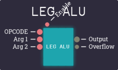
On the left we have Arg 1, Arg 2, and OPCODE. OPCODE is from 0-7
All we’re going to need though is 0: ADD and 1: SUB. Everything else isn’t going to be as useful.
Next up is the comparitor.
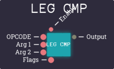
Again it has Arg 1 and 2, and a 3 bit OPCODE.
0 is EQ, 1 is NE, 2 is LT, 3 is LE, 4 is GT, 5 is GE, and 7 makes the chip output a 1 always. 6 is unused, and later on we’ll find that most of these will be unused.
If the Flags pin is set to 1, then the comparisons become signed instead of unsigned.
I am going to have to quickly make 16 bit versions of these chips though, as these are all 8 bits and we’re wanting to build a 16 bit machine.
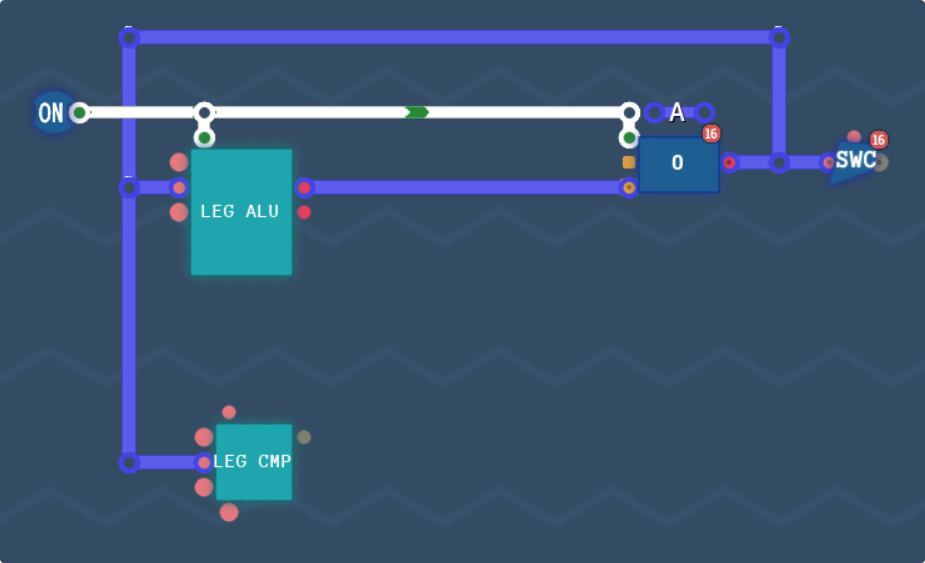
Going to sidestep some wiring and use the accumulator as an accumulator.
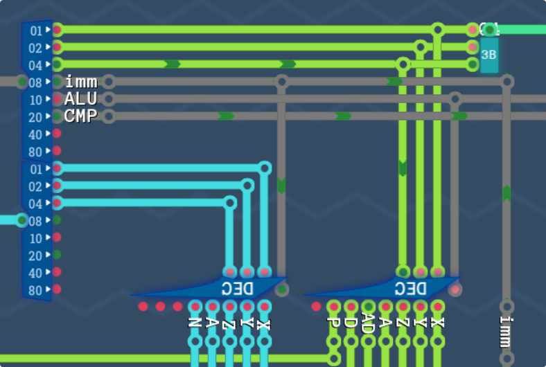
MOV instruction.
We’re gonna want some addressing modes, We have 4 registers, A, X, Y and Z, and three write-only outputs, P, AD and PPU.
- A is our accumulator.
- X, Y and Z are general purpose registers.
- P is our program counter. We should only write to this when jumping.
- AD is our PPU’s address line. We’ll set this up to increment every time PPU is written to.
- PPU is our PPU’s data line. We can set this to strobe the write line on the PPU whenever it’s written to, essentially treating our PPU as a black box RAM chip.
- Immediate is the last input. It just means take the input value directly and move it to the specified output. We can’t write to immediate.
I’m not following any specific architecture in the design here, I’m just kinda cobbling something together that will hopefully work.
Each instruction will be 2 words wide. The first word will specify our instruction and the output. The second word will be the input, either a register, jump address or some immediate data. We’ll have a bit on the instruction that says whether it should read an immediate value or a register.
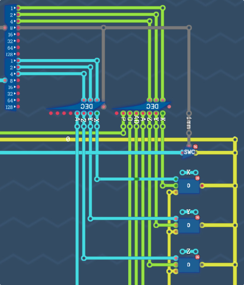
The top lines is our opcode. We’ll use the bottom 3 bits (green) to define the output, where 0-6 is X, Y, Z, A, AD, PPU Data, and P.
The blue lines is our input data. 0-3 is X, Y, Z and A. We can hook up the other lines if we need to. If the 3rd bit of our opcode is high, we’ll instead treat the blue input data as an immediate value and pipe that to wherever it’s needed.
The yellow line on the right is our general data bus. Everything writes to and reads from this, so we need to take care that only one thing is writing to it at a time.
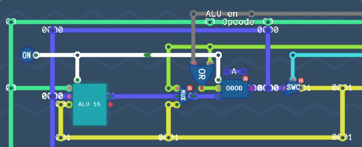
On the ALU side,
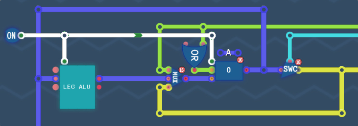
The green line as before is our destination, but we need two things to write to the accumulator, which is why there is an OR gate there. When we perform an arithmetic operation, we’ll have to save the output to the accumulator, which is why we pass through a multiplexer as well.
This one is the star of the show. It uses the AD register to store the address in PPU space that we want to write to, and more importantly, whenever we write to the PPU by outputting to the PPU’s data line, it will also increment the memory address of the PPU by 1. This means we can write a bunch of contiguous bytes at a time whilst only setting the address to write once.
Lets call the upper nibble of our movement opcode $0, so that would make our movement opcode #0000 iDDD where D is our destination, and i calls for an immediate input.
Lets test out some code shall we?
My keywords right now are simply just
x   #0000 0000
y   #0000 0001
z   #0000 0010
a   #0000 0011
ad  #0000 0100
ppu #0000 0101
p   #0000 0110
imm #0000 1000
The way that you’d write code with this, since our opcode for move is just $0X is we write the name of the register to move to first, then the name of the register to move from, or the immediate value. To set the immediate flag, we just bitwise OR it with the destination address
x|imm 1        # sets x to 1
y|imm 2        # sets y to 2
z y            # sets z to y (2)
a|imm 3        # sets a to 3
y a            # sets y to a (3)
ad|imm 0x1000  # sets ad to $1000*
ppu|imm 0x24ff # writes $24ff to the ppu data, and then increments address to $1001
ppu|imm 0x24ff # writes $24ff to ppu, and $1002 to address
ppu|imm 0x24ff # writes $24ff to ppu, and $1003 to address
And as we can see, this is exactly what’s happened (mostly, we can’t see inside the PPU memory so we’ll just have to trust for now that it worked. It didn’t crash at least.)
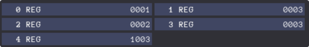
0 through 4 are X, Y, Z, A and AD respectively.
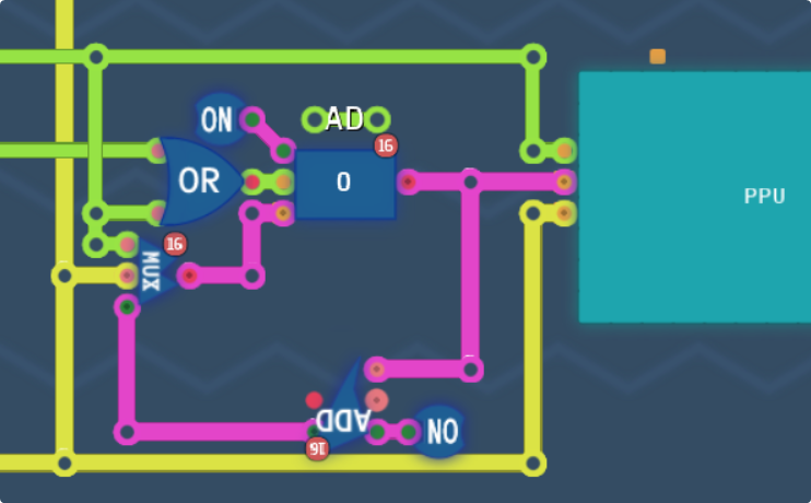
Arithmetic.
Next we’ll need to design some arithmetic functions. We already know both our ALU and CMP chips take in a 3 bit opcode, and we also know that the ALU is hooked directly into the accumulator for storing it’s output, so we don’t need to specify an output here. This means we can reuse the lower 3 bits to be our opcode when we want to do arithmetic, and the upper 4 bits can be used to decide the mode we want our computer to be in.
Lets designate #0001 iFFF to be our arithmetic functions. The immediate flag is the same, and FFF is now our arithmetic operation.
Operand 1 will always be the accumulator, so operand 2 can be the input data value/register.
The black line is our ALU enable line. We can do more logic to isolate it to a single value, but we are barely going to use 32 opcodes let alone 255, so we’ll be fine for now like this. You may have noticed that the alu is always enabled, and thats because when we want to use it, all we want to do is store it’s output to the accumulator, so there is no need to enable it manually.
The yellow bus is our second operand and is just coming from whatever data is enabled right now, and lastly we package the bottom 3 bits of the opcode into a single teal opcode line, which we’ll use both here and in the comparator. Let’s give it a test, but first, some new opcodes.
add  #0001 0000
sub  #0001 0001
and  #0001 0010
or   #0001 0011
not  #0001 0100
xor  #0001 0101
shl  #0001 0110
rol  #0001 0111
If I wanted to be smart, I could implement rotate using some system-wide carry flag, but again that’s outside the scope of this project. Perhaps if I decide to try and recreate a reasonable implementation of a 6502 (that isn’t just copying a circuit diagram into a game that doesn’t like monostable circuits.)
And again, I can bitwise OR “imm” into the code to use an immediate value.
The next chunk you’re just gonna have to trust that it works, because I’m not screenshotting every single output to post here, that’d be a bit silly…
a|imm 1    # a is 1
add|imm 2  # a is 3
sub|imm 1  # a is 2
a|imm 2
x|imm 4
add x      # a is 6
add x      # a is 10
a|imm 1
add a      # a is 2
add a      # a is 4
add a      # a is 8
shl|imm -3 # a is 1
All this works, and is good enough for me, and honestly far more than we’ll ever need. I’m sure more thourough testing would be nice, but the “expect” command only works on 8 bit machines, not 16 bit ones, which is unfortunate, and I’m not about to break this down into using 8 bit busses instead of 16 bit ones…
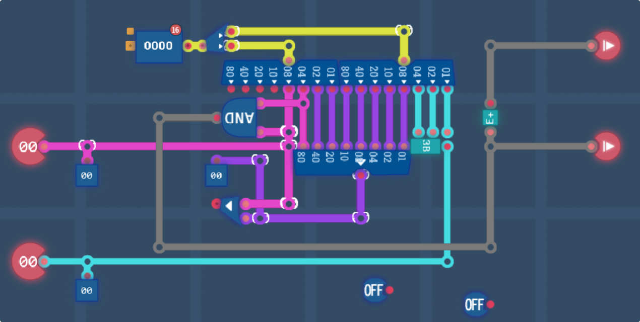
Flow Control
The last thing we need for our computer is some simple flow control. This is where our CMP chip comes into play. Again, the chip takes a 3 bit opcode, and again, we can use the lowest 3 bits of our opcode as we don’t need to store data anywhere except the P register, which we can manually overwrite by connecting the CMP chip’s output directly into the save input of the counter.
The second caveat is that we need to put the address somewhere on the data bus for the counter to read. While we could implement this exactly the same as with the alu and mov commands, the game’s bytecode editor is exactly that, a bytecode editor. So while it would be nice to have jump locations (maybe if we had a stack and call/ret commands) we won’t really need it.
Because of this we’re going to implement our jump command as #0010 1FFF where F is our CMP opcode. The reason we’re setting the third bit high is because we’re just going to output the address to jump to in the data argument directly, and this will set the immediate flag, which is perfect for us.
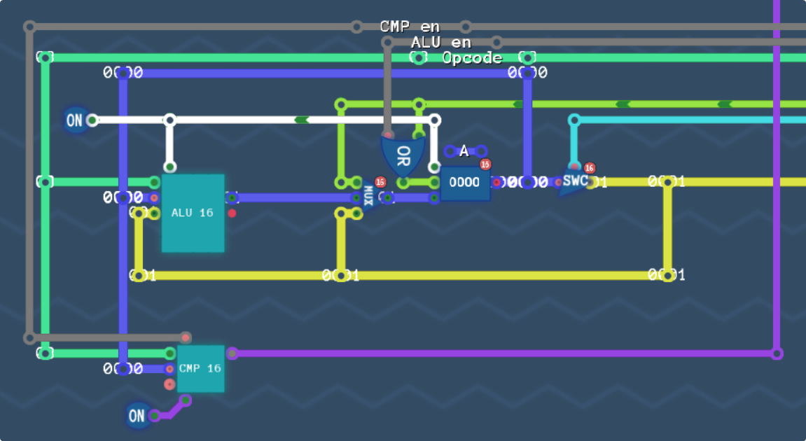
The keen eyed will notice a couple things, First we’re holding the flags pin high, and this is to enable signed operations to help mitigate the second thing, which is that the second input is disconnected.
That’s not a fault, thats just a weird design choice. Our chip does a lot of stuff, but we don’t really need all of it.
So let’s see what this crippled chip can do.
- opcode 0 tests for zero.
- opcode 2 tests for negative.
- opcode 4 tests for positive.
- opcode 7 always returns true.
This should be enough to at least let us do simple counting loops using the accumulator, it wont let us do much else though in it’s current state. We’d need a way to do a bit of maths on one of our registers to make loop testing easier. For now though, let’s run with it and see what we can do.
Lets add just a couple of opcodes.
jez  #0010 1000
jlz  #0010 1010
jgz  #0010 1100
jmp  #0010 1111
And some proof of concept testing code.
a|imm 10
label start
sub|imm 1
jgz start
This does its job, sets A to 10, decrements it until it reaches 0, then stops.
Enough Faffing Around, Draw Something Already!
On it.
So now that we have a basic computer, the last thing we need to do is figure out how to wait for the non-maskable interrupt from our PPU.
I’ll quickly set up a latch that sets itself when the NMI fires, and resets itself when it’s read.

I’ve hooked the NMI to a latch so that when it fires, it’ll be captured by the latch. The blue line at the top I’ve connected to the input “register” 4 (#0100) so that we can read from it, and reading it while it’s high will reset it to low.
nmi  #0000 0100

label wait
a nmi
jez wait
x|imm 1
This does what it is meant to. I added a halt to when the NMI fires for easier testing, and I can confirm that the CPU “spins” until the NMI fires, and then within a couple ticks, it’s seen that it has and broken out of its spinning. And also that reading the NMI buffer has properly reset it like we expected.
Now that we know when the screen is done updating, we know when we can start writing data.
Let me find that brick graphic.
Now we just need to seperate out the planes and string them together
That string on the right is our tile data.
Thankfully we’ll only need to load one of these, as our character map just has to refer to this tile over and over.
Lets get our data into the chip. Just for reference, here is our memory mapped addresses
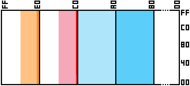
So we’ll place our tile at $8000-$8007, our colours at $C000-$C003, and then we can leave $E000-$E17F as all 0s because our tile is index 0 and our colour is index 0. Our colours are:
- Grey (Half of each component, #0 10000 10000 10000 = $4210)
- Red (Full red only, #0 11111 00000 00000 = $7C00)
- Orange (Full red, just over half green, a little blue #0 11111 10000 00111 = $7E07)
- Gold (Full red, mostly green, no blue, #0 11111 11000 00000 = $7F00)
label wait
a nmi
jez wait_

ad|imm 0x8000
ppu 0xFFFC
ppu 0xFFFC
ppu 0x00FE
ppu 0x0000
ppu 0xFCFF
ppu 0xFCFF
ppu 0xFE00
ppu 0x0000

ad|imm 0xC000
ppu 0x4210
ppu 0x7C00
ppu 0x7E07
ppu 0x7F00
This should get our data onto the chip. Lets give it a go.
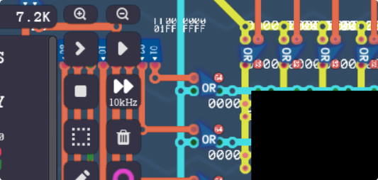
Well that didn’t work. Note the tick count being 7.2k, that mean’s we’re on the second frame. I expect the first frame to be black as no data is there yet, but we should have bricks now… Time to add some watches to the chip.
Annoyingly I cant add probes to the front of the chip, so this isn’t as intuitive as it could be, let me try and explain though.
On the left, we have 3 lights. The top one is character RAM, the middle is tile RAM, and the bottom is CG RAM. At the top is two more lights. The one near F-blank indicates that some form of blanking is happening and we can write to the chip. The one near NMI is indicating that we’re specifically in V-blank.
On the right near the row and column is the screen number.
In the middle, the top row is the current tile ID and the tick number. The middle row is the current byte of the tile being loaded. The bottom row is the 4 colours we’re using.

Well theres the first problem. We’re trying to address $8000, but it’s turned on the CG RAM chip, which isn’t what we want. If you check the diagram above again, $8000 should be the tile map. That means that the VMM chip is broken. Lets go fix that now.
Still not drawing but I spotted the issue for the second one quite easily, in fact you can see it in the screenshot above. For some reason it’s trying to write $0000 into $8004, when we programmed it to write $FCFF there. That means my code is wrong, and in fact it is. I’m not using the immediate flag so it’s just sending garbage data and disconnected registers to the chip instead. Let me add “|imm” to all my “ppu” calls.
So,,, Several things went wrong here.
First lets discuss that black square in the middle. What happened here is that our screen counter continued to tick up during V-Blank, and turns out we can’t just rely on overflow behaviour when we’re not using a power of two ticks to draw, so we ended up starting off from about a third of the way down the screen when we drew our second frame.
Lets add a reset pin to the drawing chip to reset its screen counter and see what happens next. We’ll have to trigger the reset on the falling edge of V-blank. I knew I made these “E-” chips for something.
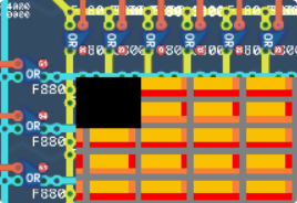
Now we seem to be off by a couple.
One other observation I had though is that it seems like we’re drawing black tiles to the screen during V-blank.
Maybe instead of resetting the counter, we should try and make it stop drawing completely during V-blank instead of just blacking out the output. I also went and fixed the typos in the tiles that I coded in tiles that are making the come out wrong. I was accidentally swapping the bytes not the nibbles, but thats sorted now.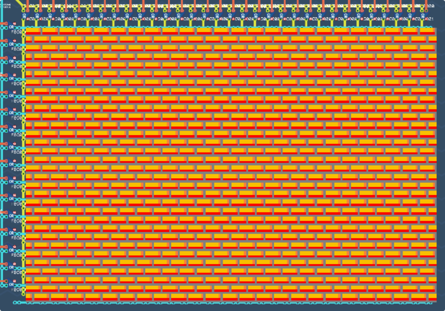
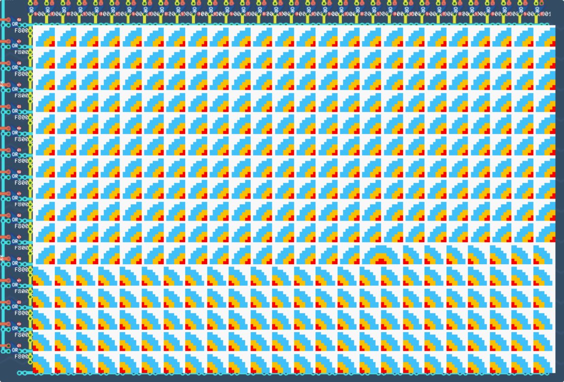
Holy shit we did it!!!
Testing the Tile Flip Bits
Lets test the flip flag next. I’ll define one tile and use the flip flag to try and print circles on the screen.
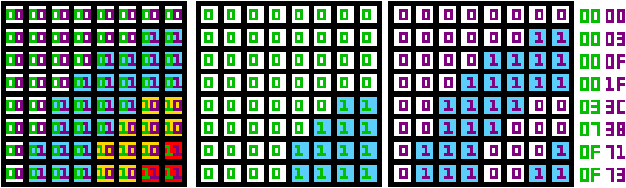
This one is gonna be a bit more of a pain to load because I’ve actually gotta write out the character map now. I can do some looping to help, but it’s not going to be fast or elegant. I’d need a better programming language or access to static ROM to make things easier. My colours this time are
- White $7FFF
- Light Blue (some red, most green, all blue, #0 01000 11000 11111 = $231F)
- Yellow (we’ll use the gold from before, 7F00)
- Red (just red, nothing else, $7C00)
Let me show you what my code is to dump all the data onto the PPU. Strap in, this is gonna be a bit tricky
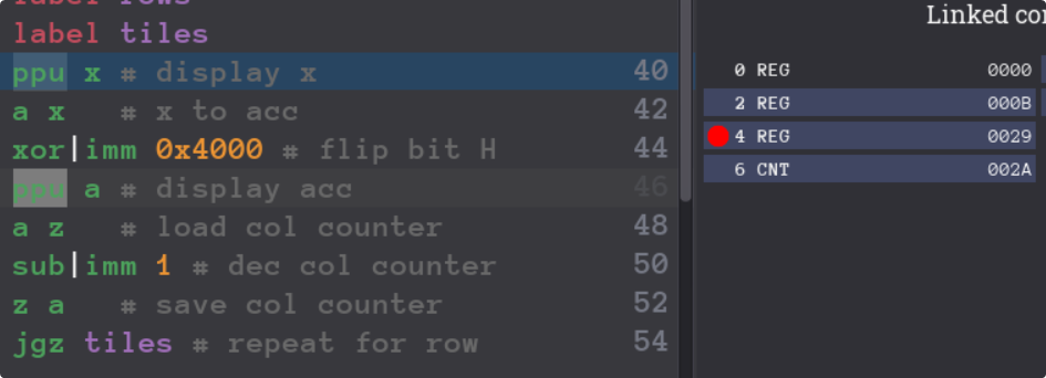
label wait  # Sleep until NMI
a nmi
jez wait

ad|imm 0x8000  # Store our quarter target block
ppu|imm 0x0000
ppu|imm 0x0003
ppu|imm 0x000F
ppu|imm 0x001F
ppu|imm 0x033C
ppu|imm 0x0738
ppu|imm 0x0F71
ppu|imm 0x0F73

ad|imm 0xC000  # Set the colour palette
ppu|imm 0x7FFF
ppu|imm 0x231F
ppu|imm 0x7F00
ppu|imm 0x7C00

ad|imm 0xE000  # Prepare to write character data
x|imm 0        # value for ppu on row
y|imm 16       # row counter
label rows
z|imm 12       # col counter
label tiles
ppu x          # display x
a x            # x to acc
xor|imm 0x4000 # flip bit H
ppu a          # display acc
a z            # load col counter
sub|imm 1      # dec col counter
z a            # save col counter
jgz tiles      # repeat for row

a x
xor|imm 0x2000 # flip bit V
x a            # update X with flipped bit
a y            # load row counter
sub|imm 1      # dec row counter
y a            # save row counter
jgz rows       # draw next row.
Essentially my code is alternating between printing $0000 and $4000 using a simple loop, then at the end of the row, it flips the 13th bit, so it then alternates between $2000 and $6000.
Well that’s concerning, the jump instruction seems to have updated the address register, what happened there?
That’d explain it. While the ALU operations disable the output address, the CMP operations don’t. Nothing a quick OR gate can’t fix fortunately. It looks like it was outputting the address of the instruction into AD instead of leaving it alone.
Well, this isn’t what we were going for either… What happened?? Starting two thirds down the screen feels a little sus, maybe its to do with clock overflow again? I don’t know…
I’ve checked that it’s writing the right values to the right places, and it looks like that is the case,
What the heck?? Was this always the case????? Why is it outputting only pin 11? Did I break this when I went to add my strobes? Or was I just that blasted at 3am on Friday… Checking back on Friday’s post, yeah I’m just dumb I suppose. It worked for us initially because we were just drawing the same tile everywhere anyway. Let me fix this real quick.
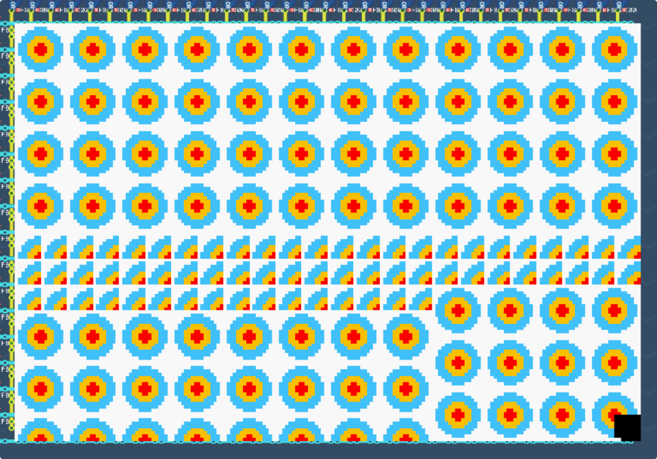
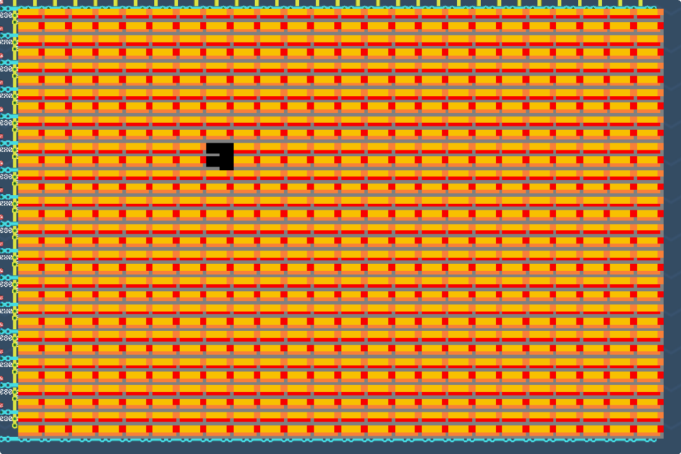
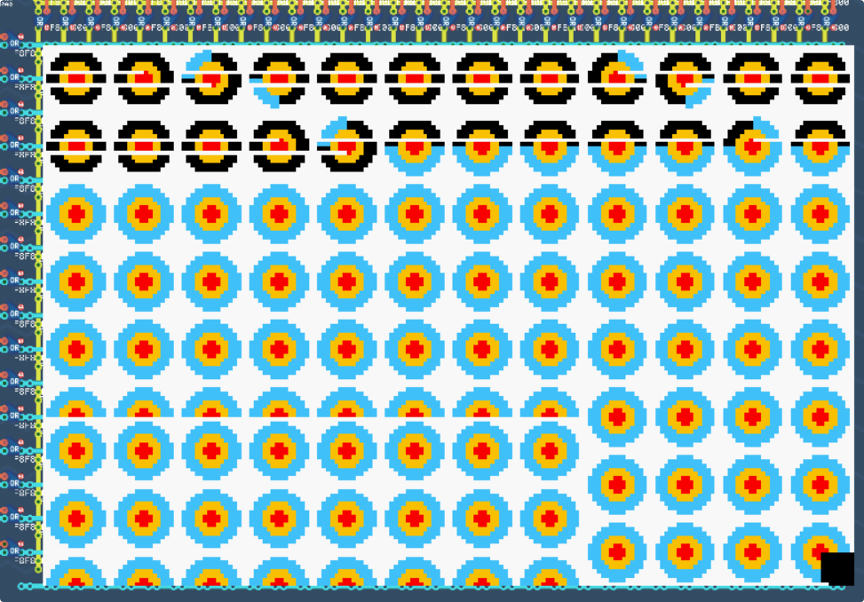
This looks a bit more promising, what happened in the middle though? 64 tiles just inexplicably broke for some reason… Ignore the artifacts in the bottom corner, it takes an extra 8 ticks after NMI to finish drawing. NMI just fires the earliest time that RAM can safely be written to.
It looks like as soon as the tile counter hits $00C0, the tile ID gets stuck as $0000, when I’d expect it to be alternating between $0000 and $4000. And that seems to go for 64 tiles, which would be up until $0100, so something weird is happening in the middle. Lets take another look at the control circuit and see what it’s doing between clock times of $0600 and $07FF…
Turns out it was doing nothing wrong, it was working as intended. The weirdness is actually coming more from the fact that there was a small bug in my script and it was only writing data up to $00C0, not up to $0100, but why did it start working again after $0100 if there was no data there? Spooky…
Thats not good,,,
Looks like it couldn’t finish writing to the PPU before V-Blank finished, so a bunch of stuff got corrupted.
I’m going to “optimise” my code a little bit, mostly by unfolding the inner loop.
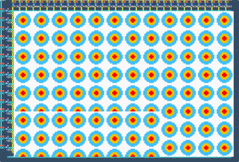
That definitely fixed the corruptions at least. Now the last thing to figure out is why it seems to be a bit broken in the bottom third. It looks like the corruption starts on tile $0100, so maybe there is some rollover issue happening, sounds like truncation perhaps?

Indeed it was truncating the tile ID. Sending a 9-bit number through an 8-bit output doesnt work oops.
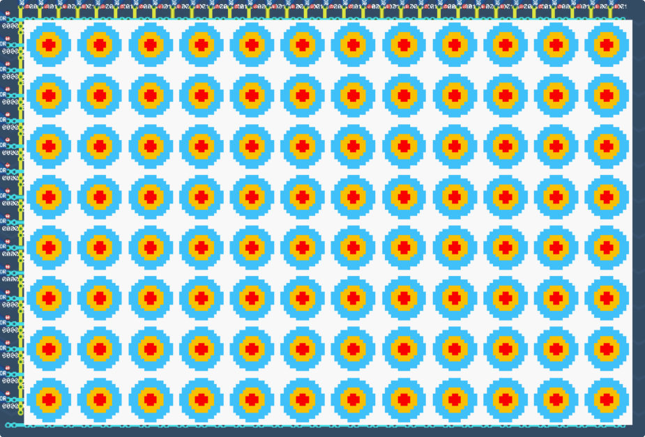
It works!!!
This time we know it works better than last time too!
The last thing to really test is if the tile map stuff actually works properly, which means I’m gonna have to dump a lot of data into the chip possibly faster than 1 V-blank cycle will allow. This is why we have F-blank, since turns out that writing to the chip without holding F-blank high will corrupt the output.
Let’s Try Drawing a Proper Scene
Most of the setup is gonna be much the same as before, so I’m not gonna go too deep into the graphics, I’ll trust that y’all will be able to convert the graphics into the bitplanes to figure out what data I’m sending to the PPU.
Here’s the tiles I want to use. I’ll do the conversions to data.

I’m not using 16×16 tiles here, screen too small for it lol, so you get low quality reductions.
234 bytes of code later, and we now have:

Nice to know that my drawing code both works, and works with non zero palettes!
Next up I’m going to just draw out a scene.
Unfortunately without massive upgrades to the computer it’s not gonna be able to do anything more than just render a frame, but oh well, it’s good enough for me for now.
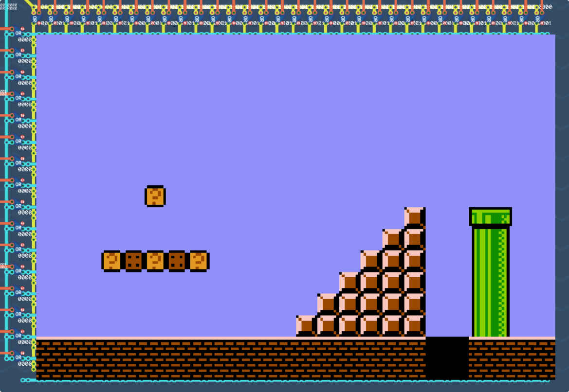
I did it! I made it draw something. My partner’s immediate response was “good job you drew cat mario” but idc because it draws something and I’m super proud of it.
Editor’s note: Partner has no idea why she said this.
I think I’m gonna stop working on this GPU for the time being. Next time I come back to this project, I’ll see if I can do scanlines instead of tile-by-tile drawing, so that I can implement more neat stuff like layers, colour maths, objects/sprites, and H-blank.
I’ll upload both the graphics driver and the GPU to the schematic hub.
- To get the PPU, search for “Basic PPU” and find the one by Lanterns.
- To get the driver, search for “Basic PPU Screen Driver” and find the one by Lanterns.
If you’ve stuck with me this far, thanks for reading. I’m sure I’ll be back on my bullshit later, but for now I’m going to take a really long rest.
If you haven’t read them already then what are you doing lol here are the links to part 1 and part 2.
Leave a Reply