Or in other words, how I’m going to make a new PPU that draws in scanlines instead of tiles.
Now, the last PPU was cool and all, honestly impressive that it even works, and can be quite succinctly summed up by one of the responses I got on the Turing Complete Discord about it, which simply said “WOW”, but let’s face the music and realise that it’s not exactly the most elegant solution. The drawing algorithm is clunky and difficult to modify the interface is actually reasonably alright imo, but overall the system is super difficult to work with.
Screen scrolling would only be possible in steps of tiles, and by overwriting the whole character map, and trying to do any additional calculations that werent just nifty wiring tricks on the source tiles would be difficult to say the least, so let’s see what we can do to make this better, shall we.
Inputs And Outputs
So what we want to output is incredibly simple. We already know what our screens take, so we can just work with that again.
For more information on this, see part 1, but in short we have 3 main outputs, Pixel, Colour and Screen.
In terms of inputs though, this is gonna rely on what features we want to try and implement on this attempt. I have some ideas what I want to try and achieve though, so let’s go through them here.
- PPU Space Data Bus
Or B-Bus (Where A-Bus is the CPU space bus.) All the changes we’re going to want to make is going to necessitate a lot more data to be stored on our PPU, as well as the PPU itself requiring exclusive access to the data bus during operation for a reason I’ll explain further down in this list. For this reason, we’re going to need a way to interract with the PPU data bus from CPU space.
If you think about it, we’ve already done this in the original chip, by having a 16 bit address and write input to write to the seperate memory modules inside the PPU, so this shouldn’t be too hard to tackle.
- Scroll Registers.
What use is a screen if we can’t smoothly scroll it. I want two registers that will control the x and y scroll offsets from the top corner of the screen. This will affect how we track and read in the data into the new screen driver we want to build. We’ll have to keep track not only of what tile we’re on, but also what line within a tile, and what row of tiles. The other implication of this is that our character map will no longer be able to be 384 characters wide, as that’d leave no space off the screen to scroll in to, so that means we’re going to expand our character map to 32×32. This will give us 8 tiles of leeway on the left or right, and 16 tiles of leeway on the top and bottom.
We’re still going to be using a 24×16 tile screen though, anything larger lags my machine too much for Turing Complete to be even remotely playable.
- Objects
We can’t really go making interesting stuff for this if we can’t have sprites that can move freely from the grid. Because of that we’re going to need a way to define and draw these sprites, or objects. We’ll decide on a definition for our objects later, and even then it might not stick, as we might discover an easier way of defining them in future. Because we’ll want to pull sprites out far faster than we’d be able to getting them one by one, we’re going to buffer all the sprite data for a row during the previous row, which should be possible to do during one row of scanning.
Our sprites will be defined with positions relative to the screen, not to the background. This means we can calculate which sprites should drawn on each scanline. We’ll allow our little PPU to keep track of 32 sprites, and our sprites are going to be 4BPP.
- Layers and Graphic Modes
I’ve not done any of the maths on how much data we’re going to be able to fetch at a time, but let’s still try and be at least a little bit reasonable about it. Every pair of rows we get for a tile will take 1 read on the address bus, and will be able to sate us for 8 draw cycles give or take. The start and end will be a bit weird about it, but we should be able to mitigate this issue by “drawing” whole tiles partially off the screen. So if we assume that we’re gonna be able to read 8 words of data, we should be doing pretty fine. If we want to use a shared data bus for tiles, colours, and characters, however, things might get a little more sketchy. Let’s see if we can stick to our 3 RAM chip approach for the time being, and use the B-Bus for the thing below.
But before we get there, let’s talk about layers and drawing modes. I don’t intend (yet) to do any of the extra features that come with chips such as the S-SMP, like offset change per column, H512, or mozaic modes, but I do want to define a few different layer modes for drawing.
I want our chip to have a 4-layer mode with the layers being 4, 2, 2 and 2BPP; a 3-layer mode with 4, 4, and 2BPP layers; and a 2 layer mode with 8BPP and 2BPP layers. Each of these modes would require reading at most 10 bitplanes from the tile data every time a new row is fetched, which is 5 reads from memory, leaving us with 3 extra reads every 8 pixels to work on other things.
- Off Board Memory
One of my biggest peeves with trying to program for our old chip is that we had to dump all the tile data into the PPU. This could end up being super slow if we needed to put in a whole huge tile map. Imagine how much faster making data available on the PPU would be if our PPU chip had address and read outputs, and a data input that we could connect to an offboard ROM chip!
This would essentially divide our tilespace into 2 different components. We’d have 512 tile entries that were saved to the PPU directly, and an additional 512 tiles that could be fetched from an external ROM chip. If we needed more than 512 tiles, we could also add an intermediate memory mapper with its own selection register and allow the CPU to do page switching during execution to swap out what tile banks are available to the PPU for a given frame.
- H-Blank Memory Access
We’re going to have some buffers that to work properly are going to need to be updated during a frame. I can’t see how we’d be able to do this sort of synchronisation between the B-Bus and A-Bus, so without doing a whole lot of research, we’re going to need a place to store our HDMA tables. Our screen is 128 pixels tall, so our HDMA tables are gonna need to be about 256 bytes (128 addresses in our 16 bit environment) each, assuming all the buffers we write to are write-once (they will be.) Theoretically we could optimise this by having tables that are capable of waiting between lines, but for now lets just assume each entry refers to one line.
We’ll need to set aside 4 pages of our address space to hold 8 HDMA channels, as well as a register that enables them.
- Colour Math
This one is probably the biggest one to think about. Basically the main issue to having multiple layers is that we need to decide which colour to write to each pixel. In our 1 background layer mode, this is almost done for us, but in all the other modes, we’ll have to think about how we get this one colour. Thats where colour math comes in. This is going to be a subsystem that takes in all our layer data and a set of registers that decide how to process that data. We aren’t going to be using 256 registers here, but we’d be best off to set a page of our memory space aside anyways as it might make wiring easier to keep all of our registers on the same page.
Memory Mapping
Lets take a quick look at what we have in our current PPU:
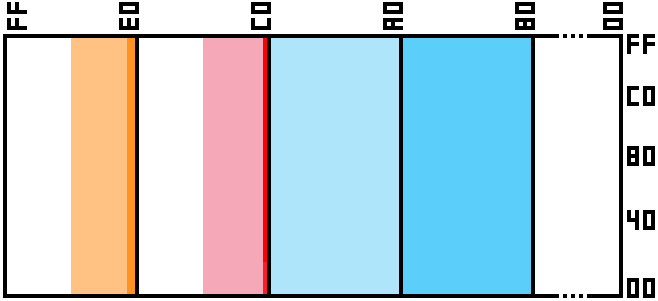
Where blue is our tile data, red is the palette, and orange is the character data, and this diagram is drawn to scale, with each pixel being 1 page wide, and 4 bytes tall.
We’re gonna have to expand this quite a lot, and also think about how we want to lay out our bitplanes. We definitely need to keep our tiles as contigious chunks in memory, and we definitely want to leave our tiles as interleaved bitplanes. This means we may be able to store our higher BPP tiles as pairs of bitplanes, strung together.
For example, We’ll have $AABB $AABB … $AABB $CCDD $CCDD … $CCDD for a 4BPP tile. This would mean that for 4BPP tiles, the offset for a tile is 16, and for 8BPP tiles it’s 32. It also means that when loading a row from a 4BPP tile, we need X and X+8, and for an 8BPP tile, X, X+8, X+16 and X+24. This isn’t awful, we can work with this.
Now if we want to consider how to lay out our memory, we’re gonna also need to take into account memory addresses to offboard ROM images, which also means we’re gonna have to divide our tile space in half. Let’s keep it simple and put the lower 512 tiles on the PPU, and the upper 512 tiles on external memory, this allows us to switch using the upper bit of the tile ID.
We’re also going to expand into the whole of memory space for this.
1024 tiles with 8BPP graphics is going to be 32768 words of data (each tile is 4×8 words.) That’s $8000 memory addresses maximum.
The other consideration is how we want to map our graphics in the lower BPP modes. It seems both inefficient and difficult to use if we were to force every tile to be 32 words long regardless of the tile depth, not to mention memory inefficient, so we’ll break our tiles out like this:
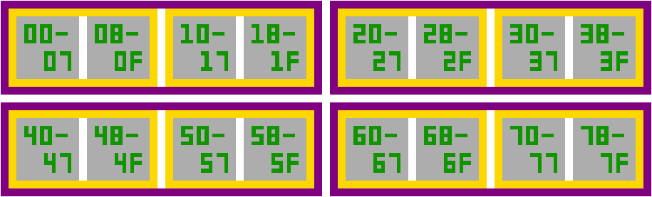
Each grey square represents a 2BPP tile taking up 8 words of memory. In 2BPP mode, each of these grey squares would be an individual tile ID. On 4BPP layers, each gold box with 2 tiles would form a single 4BPP tile, and therefore, each individual tile ID would contain 2 tiles worth of memory. Likeways for the 8BPP layer, each purple box with 4 tiles would form a single 8BPP tile.
This has the side effect of locking off some areas of the tile data exclusively for higher colour depth modes, as only the first 1024 tiles will be used in 2BPP, whereas 4BPP needs 2048 tiles, and 8BPP needs 4096 tiles, and just to double check our maths, 4096 tiles x 8 words = 32768 words.
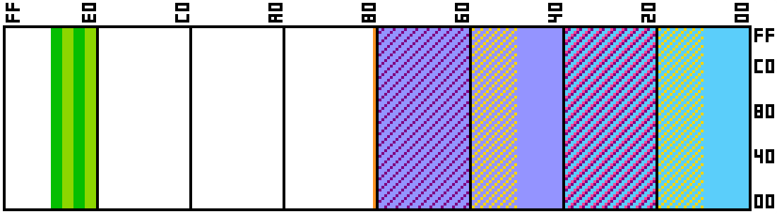
Since we want to split our memory between on and offboard memory, we’ll assign each memory chip 512 tiles, meaning that the top 512 tile entries will be used for 2BPP, 1024 for 4BPP, and 2048 for 8BPP. Let’s draw up a new memory map and assign our tile data.
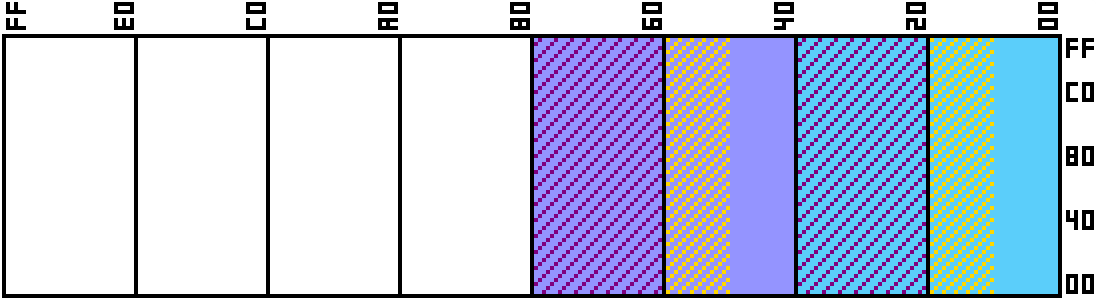
The blue section will be our memory addresses for the internal RAM, and tile IDs 0-511, and the purple area will be for the external ROM image, and associated with tiles 512 through 1023. The areas highlighted yellow will only be used in 4 and 8BPP layers. The areas in purple are only used in 8BPP layers. The nice thing about this is that with some clever use of tilemap space, the IDs 0-511 can be used on a 2BPP layer to access the top quarter of tile RAM, and the tile IDs 256-511 or 128-511 can be used by 4 and 8 BPP layers respectively in order to have a section of memory for higher fiedelity graphics that doesn’t interfere with the tileset for the lower fieldelity layers. I’d say the same logic applies between 0-511 4BPP and 256-511 8BPP, but we have no graphic modes that use both 4 and 8 BPP at the same time.
One thing to note. There is nothing stopping the external ROM from implementing bank switching (during F-blank hopefully) but I’ll leave that to the user. As long as pages $40-$4F (or $5F or $7F) contains valid tile data, I don’t care how it got there.
One other consideration is that Objects are also composed of tiles. It’d be nice if we could have seperate tile palettes for our objects than we do for our graphics, especially in modes where the 8BPP chunk of memory would otherwise be unused.
Designing Our Objects
Just like tiles are defined using a character map, objects are defined using object attributes. This is a chunk of memory that define the X and Y positions of an object, and details such as what tiles it should be drawn with and what colour palette to use, what size it is, and what priority it should be drawn with.
Let’s define an object using this form.
We’re going to want to have the object Y position on it’s own byte to make it easier to compare with. We have 128 scanlines, so we’ll use a whole byte for the object Y position. This’ll provide us some space off the bottom of the screen to hide unused objects in.
During evaluating the scanline, we’ll have to inspect these Y positions to discover which objects are going to be visible on the next scanline, then we can prepare a number of objects (8? 10? 16? I don’t know yet what our limitation would be here) that we can factor into the drawing routine for the next scanline.
Next, we’ll need the X position of the object, which our screen is 196 pixels wide, so we’d be best making this a full byte as well.
Lastly we’ll need attributes. A tile ID, a palette, a priority switch, and maybe some flip registers though it might be a little more difficult drawing flipped tiles if we’re only reading 1 line of a tile at a time, so let’s skip this part to begin with.
This leaves our data format as #000PPCCC TTTTTTTT XXXXXXXX YYYYYYYY, where Y is our Y position, X is our X position, T is the tile ID and hold your questions for just a second, C is the palette ID, and P is the priority toggle.
Let’s add objects to our memory map. We’ll want to have lets say 64 sprites for our PPU, each object is 2 words, so this is 128 addresses. Like the character map and palette, we’ll want our object attribute data to be in a seperate RAM block for speed of access, but we can probably get away with sharing the tile data here.
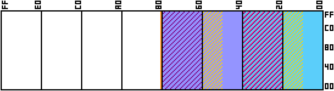
Here are the two changes. First I’ve added our object memory on page $80. We only need 128 addresses, but our wiring will be easier if we just allocate the whole page, and second I’ve designated the second quarter of tile memory to be for sprite tiles. This is why the tile ID is only 8 bits long in the definition above, because 32 pages of memory is enough to store 256 tiles at 4BPP. My reasoning for doing this is that I suspect it’s going to end up being more desirable to use the 3 or 4 background modes rather than the 2 background mode, and therefore a lot of the time, the purple striped areas of memory won’t ever be used, therefore by allocating our object tiles to the upper half of onboard memory, we can fully utilise the onboard memory for all the object tiles and half of the common background tiles.
We may be able to handle more than 64 objects, but lets start off with a reasonable amount. We’ve got to scan this table every scanline anyway.
Mapping Maps
Next thing to consider is layers. I want to continue using the same format as before, though to begin with I’ll be dropping support for flipping tiles vertically. On the other hand we’ll now be able to use the priority bit. If you remember from part 2, the format is #PHVC CCTT TTTT TTTT, where P is for priority, H and V flip the characters, C is our palette ID, and T is the tile ID.
Our new tile maps are going to be 32 tiles wide and 32 tiles tall, which is a damn sight larger than our existing layer. This means that it’s going to take 1024 characters, or $400 addresses (4 pages) for each layer, and we could have up to 4 of them.
We’ll map these to the top of our address space just like we did before.
Nice and simple. 4 bands of 4 pages = 4 layers, what more is there to say. Of course we’ll only actually need all 4 layers in the 4 layer mode, but that’s besides the point.
And while we’re here, we may as well finish off our chart and fill in the last couple of pieces that we’re going to need to map that isn’t just a stack of registers scattered around the place.
First up, we’re gonna need a full 256 bytes of colours this time, as well as deciding on how they’re allocated into palettes.
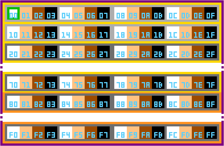
Like in the graphic above, grey indicates 2BPP, gold is 4BPP (both tiles and sprites), and purple indicates 8BPP, and just like in our old computer, the 2BPP mode only needs 32 colours. Here though, we’re going to use 256 colours for our 8BPP palette. This gives us 64 2BPP palettes, which is utterly absured, and also why starting at $20, I’ve greyed out the grey boxes to indicate that they are no longer 2BPP colours.
At 4BPP however, we get 16 palettes, which we can evenly use between background tiles and objects, as each category requires 8 palettes each, which are designated by the gold and orange boxes. Perfect fit!
At 8BPP, objects and backgrounds are gonna have to share though, and regardless of the mode, the first 32 colours are gonna be shared with the 2BPP layer regardless.
Colour $00 is special, its going to be used as the background colour for the whole screen when nothing else is displayed. How can nothing else be displayed? Well colour 0 for every palette now is no longer going to be whatever colour is in that location on the palette, but rather fully transparent.
And the last chunk of memory we’re going to need are our HDMA tables, which we aren’t actually going to implement as Direct Memory Access (DMA) but rather as just a set of scheduled writes that the PPU is going to handle during it’s H-blank period.
Each frame has 128 scanlines, so our HDMA tables need to update 128 values. We’ll reserve 8 pages just in case it does ever come up that we end up using write twice buffers for anything, but with a 16 bit data width, I doubt that’ll ever happen. It will make wiring easier though.
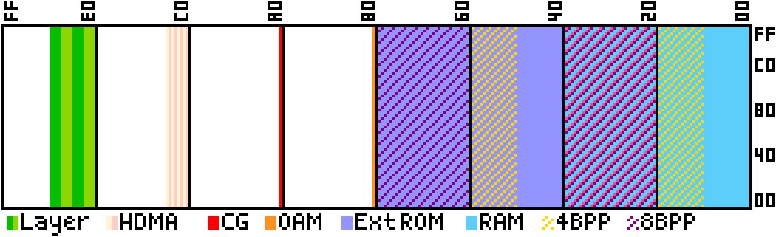
Red is our 1 page of colour graphics at $A0, and yellow/pink is our 8 HDMA channels at $C0-$C7.
The last thing we’re gonna need is addresses for all our hardware registers.
Let’s Think About Colour Math
The main benefit to drawing our outputs one pixel at a time is that it let’s us make decisions about how each pixel should be drawn based on a set of inputs and configurations. So let’s talk about the configurations and how this should work.
Now I’m not going to completely rip off the S-PPU’s colour math settings, I will be taking some inspiration in how I want our chip to work. For those not wanting to watch a video though, how it works is that it first divides the layers between two screens, a main and sub screen, then uses a pair of windows to select whether a layer should be displayed on the main or sub screen. Then after some ordering between the layers to decide which pixel is on top, colour math finally maths the main and sub screens together either by addition, subtraction, or averaging.
Lets try and figure out what information our colour math is going to need.
- Colour math enable (background)
- Colour math enable (objects)
- Main screen enables for each of the layers.
- Sub screen enables for each of the layers.
- Main and sub screen blanking.
- Math mode.
- Priority mode. – The SNES decides whether to place the high priority layer 3 above or below layers 1 and 2, and the object layer.
- Window start and end registers for each window.
- Window enables for each layer on the main and sub screens.
- Window selection modes for each layer on the main and sub screens (and, or, nand, xor)
And lets create a pipeline, like I said, I’m not going to completely rip off the S-PPU, but I am gonna follow a fair bit of it, so lets design a pipeline, though the more I look at it, the more I want to implement this pipeline wholesale tbh… So I guess in that regard, let’s go through how the colour math works, and see how much of it is feasable to do.
- Enabling the two windows per layer
Doable, we should do this
- Inverting the windows per layer
Should probably do this to make sure windowing works
- Window combinatorics
Yep, we can do this too.
- Layer data onto main and sub windows
Yeah this is possible
- Masking using windows on either layer
Totally possible
- Seperate designated colour for the sub-layer
- Option to choose this colour specifically
- Option to cull entire screens based on the window
- Option to invert, enable, or disable this culling
- Enabling colour math based on which layer is on top
- Add, Sub, and Avg functions for math
Wait, is that the whole process? Well uh, fuck, I guess I am just going to be building myself an S-PPU colour math chip then, how awkward lmao. Of course there will be some considerations to work with such as how we’re using a 16 bit architecture for our PPU and not an 8-bit one, but I’m sure we’ll figure something out.
Let’s designate ourselves some registers then, we’ll just line all our registers up on page $FF.
- $00: Through Main Screen (#000J4321) 1 = put pixel on main screen. J is our object layer.
- $01: Through Sub Screen (#000J4321) 1 = put pixel on sub screen.
- $02: Through Main Window (#000J4321) 1 = mask the pixel on the main screen if outside the window
- $03: Through Sub Window (#000J4321) 1 = mask the pixel on the sub screen if outside the window
- $04: Window enables, backgrounds (#44443333 22221111) Each nibble represents the windowing mode. The first and second bits are passed to the window 1 enable and invert inputs (00 = disable, 10 = enable, 11 = invert). The third and fourth bits are the same but for window 2.
- $05: Window enables, objects (#MMMMJJJJ) Same as above. MMMM is treated as an additional layer mask that will cull away any colour immediately before mathing the output, leaving the screen transparent.
- $06: Window combine mode (#0000MMJJ 44332211) 00 = OR, 01 = AND, 02 = XOR, 03 = XNOR
- $08: High Priority Layer 3 (#P)
- $09: Sub Screen Colour ($PP) A palette index to assign to the sub screen if no pixel is visible, or if the fixed colour switch is set.
- $0A: Math Enable (#SH0J4321) 1 = math if this layer is on top. SH is the math mode. S determines if the sub window is added or subtracted, and H will half the output of the addition/subtraction.
- $0B: Mask window flags (#MMSS00C0) MM is the window mode on the main screen, 00 = pass through, 01 = inside window, 10 = outside window, 11 = disable. SS is the same as MM but for the sub screen. C disables the subscreen and replaces it with just the sub screen colour. If a screen is masked away, it’s replaced with transparency.
- $0C: Window 1 position ($SSEE) Word data where top byte is the start position and bottom byte is the end position.
- $0D: Window 2 position ($SSEE)
- Unless I find a use for them, which doesn’t seem necessary, $07, $0E and $0F remain unused.
Maybe in future I’ll remap these hardware registers to match those of the colour math chip in the SNES, but right now I’m not too bothered.
Whew thats a lot. I’m going to build this chip first though, that feels like a pretty easy place to start.
In fact, I’m only 4000 words into this post so far, let’s crack open the simulation and give it a go.
Screw it, I’m Opening Up The Simulation Again
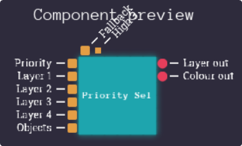
Is it weird to say I feel in my element again? Also this chip absolutely isn’t going to remain this small, there is a lot to do here, so may as well make a start. Actually interestingly enough, I’m missing a couple of inputs that we’ll require as well, so the left of this chip is about to get a lot bigger…
Well, that’s uncomfortable to read. As objects have 2 priority bits, I’ve just listed this as an 8-bit input, rather than 2 pins of 1-bit input.
This isn’t even it’s final form, later on we’re going to be adding an extra 2 address outputs, and an extra data input so that we can read the colours we decide to fetch from CGRAM, as our inputs are going to be colour indicies, rather than the 16 bit colours directly. The benefit to this is that it’ll greatly reduce the time it takes to fetch the input data at the cost of adding an extra tick of delay between when we prepare the data for colour math and when we can output it, but in the grand scheme of things, one extra tick per line isn’t going. to be the end of the world. We’re also going to need some communication pins (clock, strobe, whatever) to tell it when it can do it’s work, and to also give us a chance to disable it to write to its internal registers.
First we’ll need to set up some registers, which we decided above.
Not my best wiring, but it’ll get the job done. I’ve annotated which register is which, they’re in the same address order as the list above, but just for reference, from left to right, we have Through Main/Sub Screens, Through Main/Sub Windows, Window Enable BG/Objects, Window Logic, High Priority 3, Colour, Math Enable, Screen Mask Settings, and W1/W2 Positions.
We’ll be able to use these further on in the pipeline.
So lets make a start on our pipeline.
We’ll need a stack of switches to disable inputs on each of the lines so I’ll create a quick switch line that takes an 8 bit input and zeroes out the 5 outputs depending on the input. We’ll then leave the transparency logic to the layer selector chip.
When we need to blank out a colour for a layer, we can simply set its colour palette index to 0, but first let’s figure out if our pixels are outside of windows and need blanking in the first place.
I’ve wired up some logic for the windows:
This is part of the reason we packed the window logic controls how we did. It allowed us to run nibbles of data into our selection subchips (which are very simple logic, on the left we have P = A*En1^In1 and Q = B*En2^In2, and on the right we have either P+Q, P*Q, P^Q or ¬(P^Q) depending on the 2 bit input from the top right.) This is far far easier than trying to interlace individual bits from 4 different registers. Some small utility chips, B44 takes 1 8-bit input and outputs the upper and lower nibbles as the bottom 4 bits of an 8 bit line. P4 takes an 8 bit input and outputs 4 pairs of 2 bit values on the lowest bits of the corresponding lines.
At the end of this section, we have 5 pink lines, which are our 5 layer windows, and a purple line, which is the mask window.
This is the part of the logic where zero out the colour if either the TxS is disabled, or if TxW is enabled, but the window for that layer is disabled. If the TxW is disabled, we just allow the pixel through unaltered.
A New Day
It’s been a few days since I was last working on this, and I’ve kinda been thinking about it in passing when I figured out a key detail that might help us. Remember how earlier I said
This isn’t even it’s final form, later on we’re going to be adding an extra 2 address outputs, and an extra data input so that we can read the colours we decide to fetch from CGRAM
Well this might not be strictly true. Turns out that “CG” doesnt mean “Colour Graphic”, it means “Colour Generator”, which in theory is what we’re building right now, no? So that means if we want, we can just embed our colours into this chip instead of on the main board.
That would save us having to run an extra address and data line to the outside board, at the cost of not being able to see the colour data on the outside board.
It also simplifies our memory mapping a little bit, because my next magic trick is to move our CM hardware registers from page $FF to page $A1. The reason for this is that our CGRAM is already mapped to page $A0, so we can just check for page $Ax and route all data into the CM chip. This works because we built the colour chip to only take a 8 bit address, not the whole 16 bit address. The change we’d have to make for this is to make the input 16 bit and only enable the register writes when bit 8 is high, and colours when bit 8 is low. The list of address registers above will stay the same.
All that being said, we’re going to have to hook up our CGRAM inside the CM chip.
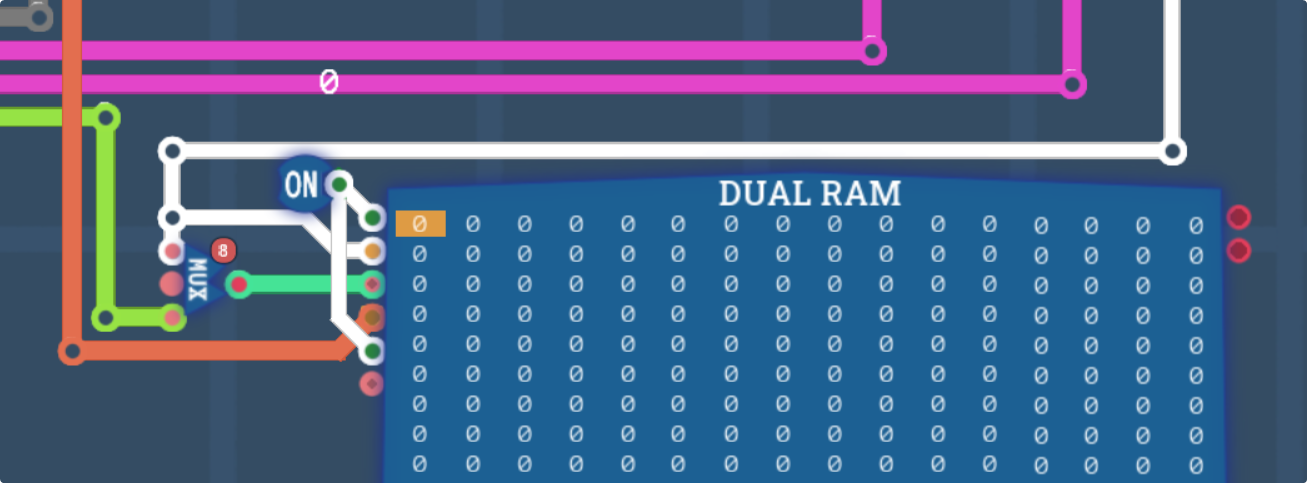
The game has a second kind of ram built into it, which is going to really help for us. We need to get two different colours out of CGRAM before doing the math part of colour math, so we’ll need to be able to fetch two colours at once.
Internally this thing is just like, this,

but in a grid, so basically it only has one write pin which is perfectly suitable for us, but we can read two different addresses at a time. That means that when we’re retrieving colours, we can take the two outputs from our priority circuits, then index into the dual-ram to get the two colours to do math on. But we’ve got a few steps to go through before we get there.
Layer priority
First up, layer priority. We have 2 screens, each with 5 colours, and a set of 6 priorities.
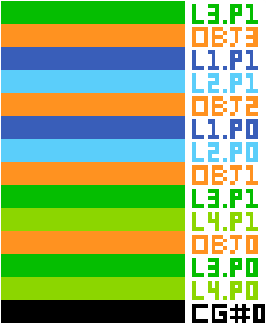
Objects can have 4 priority levels, while layers only have 2. Layer 3, you may notice, has two positions for its priority 1 layer, and thats because the switch at $B108 will move L3.P1 up to the very top of the stack if enabled. On the SNES, this only happens using its “Background Mode 1”, which is a 4+4+2 BPP mode, but I see no reason why we can’t just implement it for both of our 3 and 4 layer modes.
At the very bottom of the stack is CGRAM address $00, which if you remember from before is our background colour. This will be the fallback (for the main screen) if no other colour is available. Of course though, for the sub screen, we can actually specify a different CGRAM address to use as the fallback, assuming we don’t ultimately disable the subscreen in its entirety.
Our priority circuit is going to have to take in the 5 layers, and the priority settings, as well as an optional fallback colour, and then it’ll have to output the topmost colour, as well as what layer that colour is.
Lets think about this then.
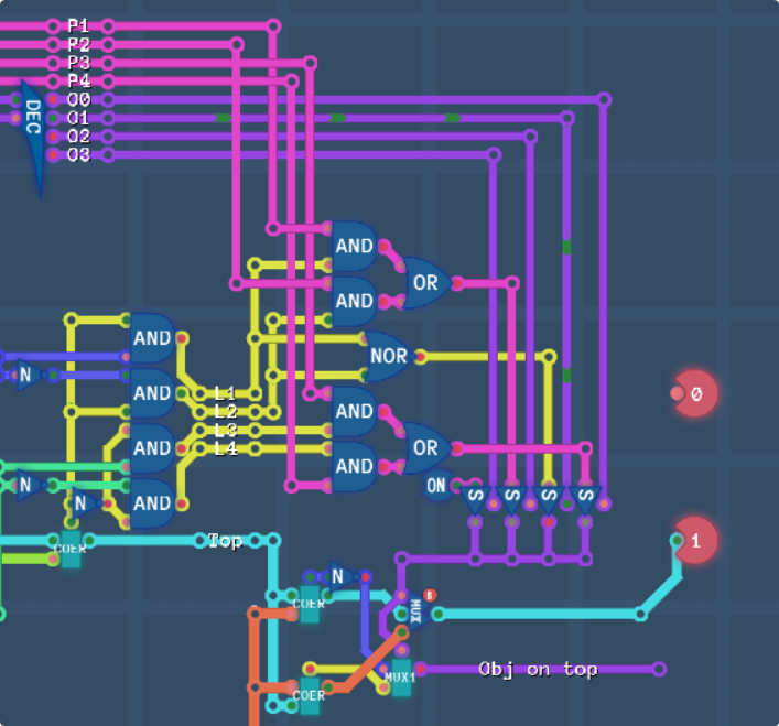
Layers 1 and 2 are in a pair, and same for 3 and 4. Therefore the only way for layer 2/4 to be above layer 1/3, is if 2/4 is high priority and 1/3 is not.
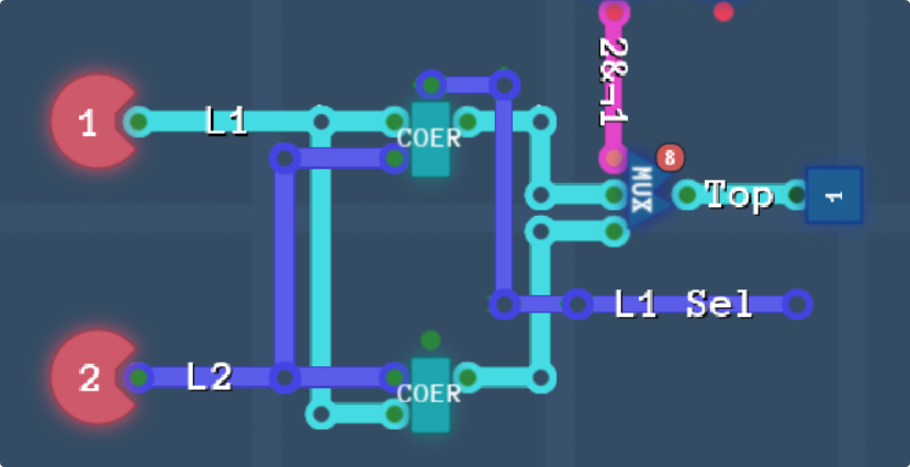
The pink line is coming from an AND gate testing for NOT L1-pri & L2-pri, and “COER” is a coersion/coalesce chip, It returns the first input if it’s not 0, or the second input otherwise. The top output is on if the first input is returned, which we’ll have to use to figure out which layer is on top for colour math later. Lastly, the multiplexer is handling the reversed layer order that happens when L2&¬L1 is high, returning L2 (if non-zero) instead of L1.
Next up is inserting the object layer. This is based on the object priority and also the priority of the other layers.
Objects with priority 3 are always on top, objects with priority 2 are below high priority layers 1/2, objects with priority 1 are always between the top pair and bottom pair, and objects with priority 0 are below high priority layers 3/4. So we’re gonna need to know the priority of the objects, as well as the priority of each layer, and which layer is on top. The reason we need to know what is on top is because if we presume that L3 is high priority, and L4 isnt, but L3 is transparent, then P0 objects still need to come out on top.
The alternative implementation is that we calculate all the layer data first, then through some absured logic as well as knowledge of what is on top, we can then calculate if the objects should be displayed. This might be easier. We’ll handle the high priority layer 3 as a final switch and coerce after the rest of the calculations. Thankfully as layers 1/2 is always above layers 3/4, we can implemente this as one coerce.

So, out the right, we now know which of the 4 layers is on top. The issue here though is that if there is no colour on any of the layers, L4 will be high, but Top will be low. Then again, this would end up being coerced into the object layer anyway even if layer 4’s priority is high.
Logic time, and we’re gonna handle each object priority seperate.
- If the object is priority 3, output the object.
- If the object is priority 2, we need to AND P1 and L1 to test if L1 is on top and high priority, then same for P2/L2, and then we OR the result of that together, which tells us if either of the two layers is high priority and on top.
- If the object is priority 1, we output the layer if L1 or L2, otherwise the object.
- If the object is priority 0, we do the same logic as for priority 2, just with P3/L3 and P4/L4.
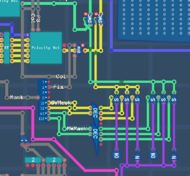
Yet another screenshot to stack on the pile of bad wiring. At the bottom is the output layer, and if the purple line is high, it means that the object layer is the one that was output. So lastly, the priority line needs to be output. For ease of the chips outside, we’re going to output it the same way as priorities are input, with 1 bit for each layer on an 8 bit line. Saves me having to encode anything. Again, some pretty tight wiring, but it gets the job done!
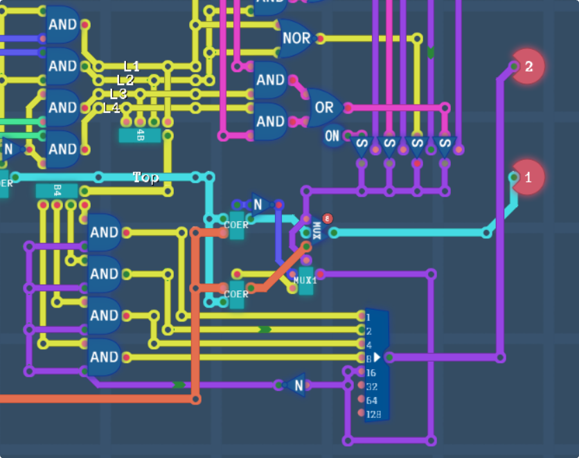
Unfortunately we’re not done yet. In the weird edge case where all the layer data is 0, this chip needs to output the default colour, and we also have the high priority layer 3 switch to contend with. And it’s gotten to the point where my wiring is a little bit too messy to work with and fit in these final components, so I’m going to take the switching circuit that is in the first screenshot of this section into it’s own priority coalesce chip.
And here’s the last step.
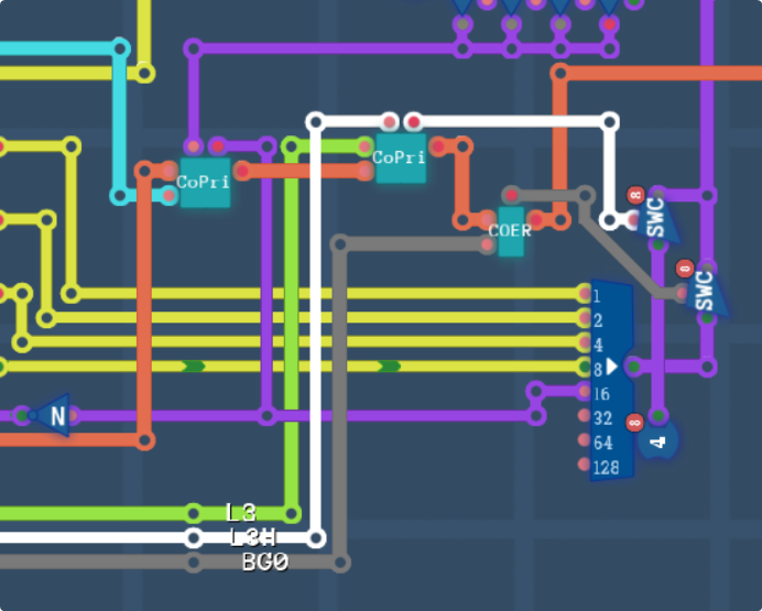
“CoPri” is just that condensed priority selection and coercion circuit I mentioned above. The 3 chips in a row, the first one takes the object and layer data and outputs whichever one is on top (as well as setting up the top layer output.) The second checks the high priority layer 3 switch to put L3 on top of anything else, as well as changing the layer output value to #0 0100, and lastly is a check to make sure we’re not outputting a transparent window, and to pass the default colour if we are, as well as setting the output layer to #0 0000.
And that’s done! We can now determine what colour is on the main and sub screens in the colour math chip.
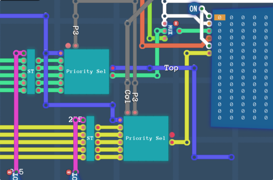
And that’s the priority select chips installed. The dark blue is the input priority bundle in the format #00JJ 4321, which is what we’re expecting in the chip. The two output colours are fed into the dual access RAM in order to get the 2 colours we need, and the top layer of the main screen will be ANDed with the colour math enable register to determine if we want to put the two colours through math.
Time to actually do the colour math stuff!
The last part before we get to doing math is adding in the fixed colour toggle, and the screen windowing modes.
Remember how there was actually 6 window layers defined, Layers 1-4, Objects and the Mask, this is the mask part. We’re gonna have to take our masking window and then set that up using the mask logic register to figure out the colour to get from RAM.
So what we have now, the purple line is our window 6 (mask/fixed colour window,) and the Mask hardware register, from which we take the fixed colour switch and the mask settings. The mask settings switch between passthrough, inside, outside and block, for both the main and sub screens. Then the output of these go into the switches to enable or disable that screen. Note that in this case, “disabling” means that colour 0 is being used, which actually now that I think about it, I went back to check and this is wrong…
It’s meant to output transparent, not CGRAM colour 0, let me fix that real quick…
There we go, this should set the colours to transparent if they aren’t needed.
Anyways, where was I?
Right, at this point, we have to unpack the 16 bit colour into components then do the math on each component individually. If one of the screen colours is $0000, then we put the other screen through unaltered, and if both screens come through as $0000 then the pixel is just black.
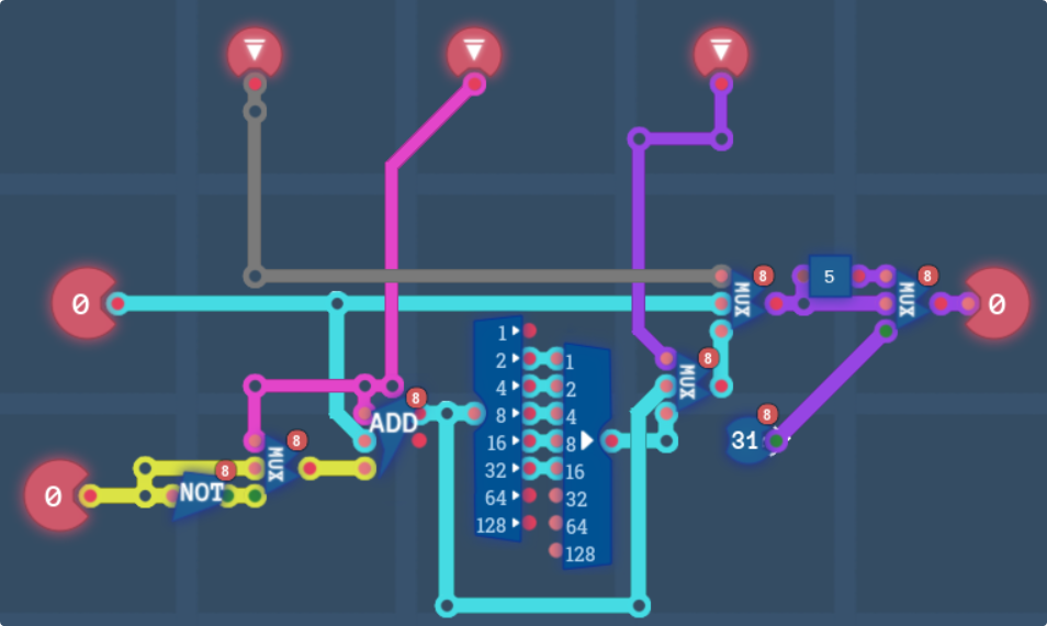
This is the logic for one channel in the colour math. From left to right, we have a multiplexer selecting between the number and the ones-compliment of it, which is switched based on the middle (Subtract) pin. Then an adder that adds the main and sub screen together, along with a +1 if we’re subtracting (to get the twos-compliment.) Next in the chain is some wiring to half the sum’s value which we switch based on the third (Half) pin.
At the end of the chain, we have 2 more multiplexers. The first one completely disables math based on the first (Enable) pin, and the second one clamps the value to 31 if it’s in the range 32-63 (which as our inputs are always going to be 0-31, this is suitable for our needs.
Next up, we just put three of these, one for each channel. This is also where we have to check for transparency. Since our channel math handles the enable pin for us, we don’t need to implement that again, just the transparency checks.
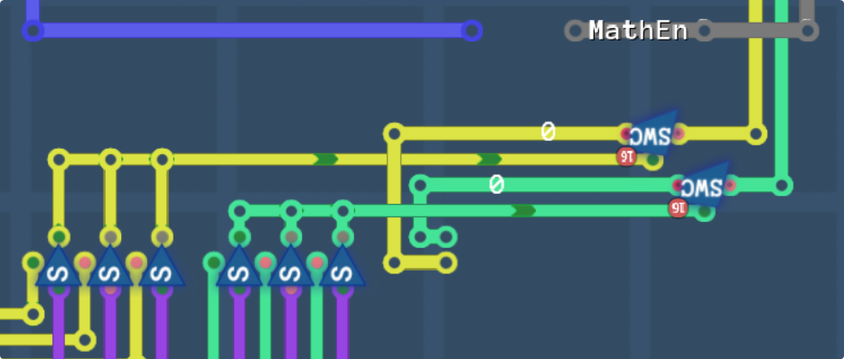
For the heart of colour math, its surprisingly simple.
On the left, we unpack the two 16 bit colours from #0RRR RRGG GGGB BBBB into 3 different 5 bit numbers, feed each of them into a channel math circuit (which does the math enable check for us) and outputs the results. N16 is just a 16 bit not-zero checker, since one-bit inputs only use the lowest bit of a line, so it just ORs all the bits together. The decoder on the right has 4 options, either both main and sub are transparent, in which case we output black, or one is transparent in which case we output the other, or both are colours and we do math normally.
Lets get this into our colour math chip!
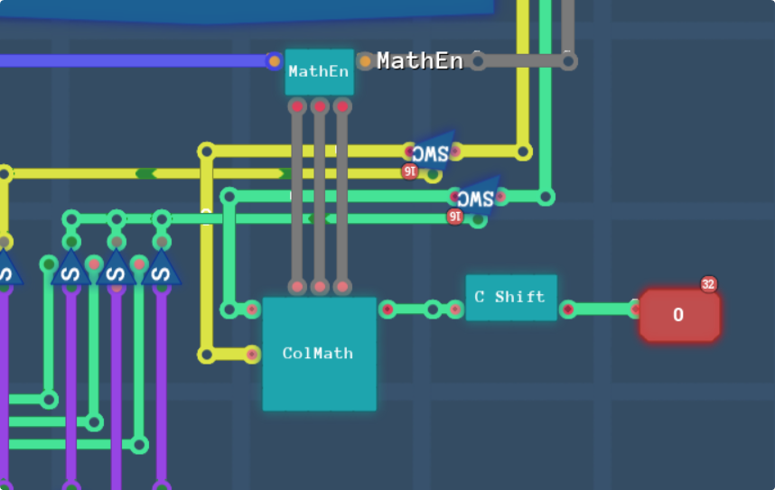
And thats everything!! The “C Shift” chip is identical to the one about half way down my first PPU post, and it just takes in our 16 bit format colour and converts it to the lower 3 bytes of a 32 bit output. They will need to be shifted up to the upper 3 bytes at some point, but I’m sure I’ll remember to do that, and if all my screens look cyan, feel free to yell at me because this is probably why lol.
Bless the mess
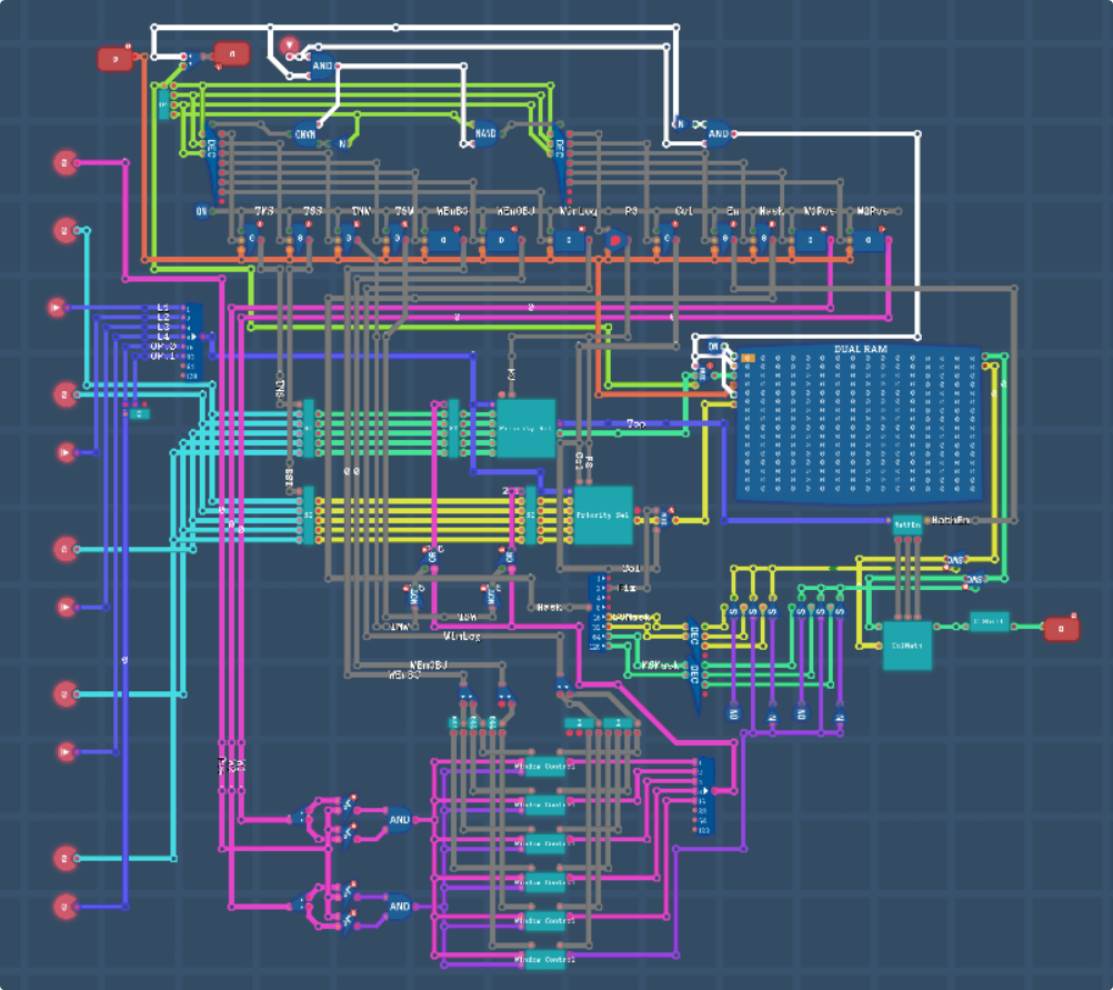
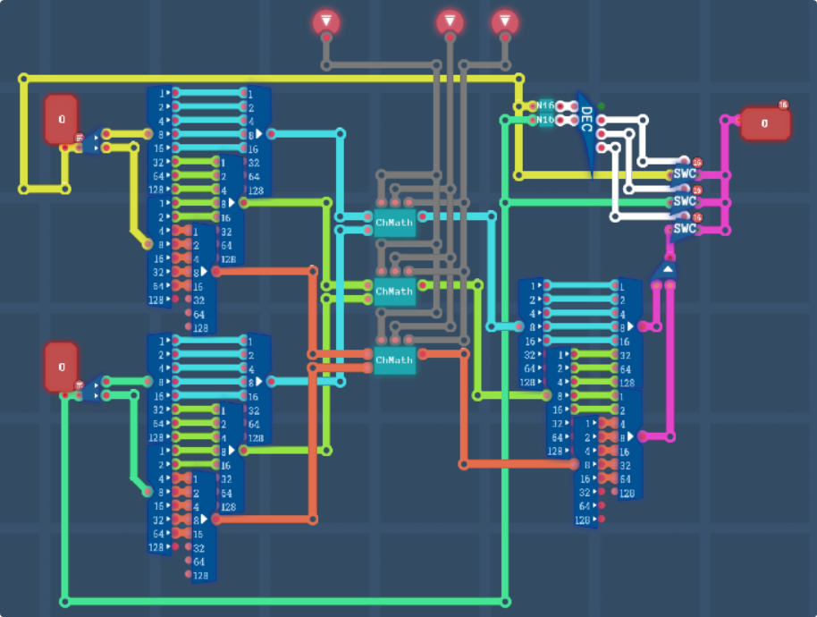
So, at the end of all of this, this is what is left. I’m sure if you want to dig deeper you can go read everything again to see the more zoomed in screenshots of each section, but for a more broad overview I’ll annotate a version below:
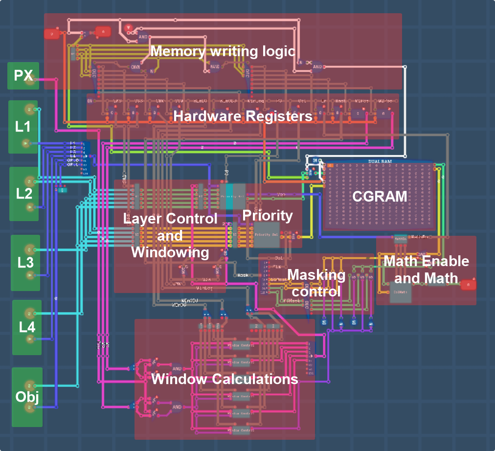
And just as a reminder for myself when it comes to memory mapping this thing, the internal memory address space starts at $0000, page $00 is entirely dedicated to CGRAM, and page $01 has hardware registers between $0100 and $010F. Thankfully this won’t be too much of a problem until I go to build memory mapping for the PPU.
Time for a nap
Sorry this one took forever to get out and was a bit all over the place. I started off just wanting to plan it, then got side tracked building the colour math circuitry, which was fun don’t get me wrong, and then ended up not having any time for like, almost a month after that, but I am also kinda dreading trying to get the timing down for the stuff outside this chip, especially like, scroll registers and what have you, but oh well I’ll cross that bridge when I get there. Hopefully next one soon? Though I don’t really know where to start with it. Maybe I’ll try and do the tile fetching.
I think when it comes to modes, I’ll literally build 3 different circuits that interface with the tilemap RAM, and send an enable signal based on what mode the PPU is in, but again I’ll worry about that later. For now, after just over 7000 words, I’m gonna go sleep.
Leave a Reply